Tag Archives: University of Texas at Austin

New electrochromic material for ‘smart’ windows

Given that it’s summer, I seem to be increasingly obsessed with windows that help control the heat from the sun. So, this Aug. 22, 2016 news item on ScienceDaily hit my sweet spot,

Researchers in the Cockrell School of Engineering at The University of Texas at Austin have invented a new flexible smart window material that, when incorporated into windows, sunroofs, or even curved glass surfaces, will have the ability to control both heat and light from the sun. …

Delia Milliron, an associate professor in the McKetta Department of Chemical Engineering, and her team’s advancement is a new low-temperature process for coating the new smart material on plastic, which makes it easier and cheaper to apply than conventional coatings made directly on the glass itself. The team demonstrated a flexible electrochromic device, which means a small electric charge (about 4 volts) can lighten or darken the material and control the transmission of heat-producing, near-infrared radiation. Such smart windows are aimed at saving on cooling and heating bills for homes and businesses.

An Aug. 22, 2016 University of Texas at Austin news release (also on EurekAlert), which originated the news item, describes the international team behind this research and offers more details about the research itself,

The research team is an international collaboration, including scientists at the European Synchrotron Radiation Facility and CNRS in France, and Ikerbasque in Spain. Researchers at UT Austin’s College of Natural Sciences provided key theoretical work.

Milliron and her team’s low-temperature process generates a material with a unique nanostructure, which doubles the efficiency of the coloration process compared with a coating produced by a conventional high-temperature process. It can switch between clear and tinted more quickly, using less power.

The new electrochromic material, like its high-temperature processed counterpart, has an amorphous structure, meaning the atoms lack any long-range organization as would be found in a crystal. However, the new process yields a unique local arrangement of the atoms in a linear, chain-like structure. Whereas conventional amorphous materials produced at high temperature have a denser three-dimensionally bonded structure, the researchers’ new linearly structured material, made of chemically condensed niobium oxide, allows ions to flow in and out more freely. As a result, it is twice as energy efficient as the conventionally processed smart window material.

At the heart of the team’s study is their rare insight into the atomic-scale structure of the amorphous materials, whose disordered structures are difficult to characterize. Because there are few techniques for characterizing the atomic-scale structure sufficiently enough to understand properties, it has been difficult to engineer amorphous materials to enhance their performance.

“There’s relatively little insight into amorphous materials and how their properties are impacted by local structure,” Milliron said. “But, we were able to characterize with enough specificity what the local arrangement of the atoms is, so that it sheds light on the differences in properties in a rational way.”

Graeme Henkelman, a co-author on the paper and chemistry professor in UT Austin’s College of Natural Sciences, explains that determining the atomic structure for amorphous materials is far more difficult than for crystalline materials, which have an ordered structure. In this case, the researchers were able to use a combination of techniques and measurements to determine an atomic structure that is consistent in both experiment and theory.

“Such collaborative efforts that combine complementary techniques are, in my view, the key to the rational design of new materials,” Henkelman said.

Milliron believes the knowledge gained here could inspire deliberate engineering of amorphous materials for other applications such as supercapacitors that store and release electrical energy rapidly and efficiently.

The Milliron lab’s next challenge is to develop a flexible material using their low-temperature process that meets or exceeds the best performance of electrochromic materials made by conventional high-temperature processing.

“We want to see if we can marry the best performance with this new low-temperature processing strategy,” she said.

Here’s a link to and a citation for the paper,

Linear topology in amorphous metal oxide electrochromic networks obtained via low-temperature solution processing by Anna Llordés, Yang Wang, Alejandro Fernandez-Martinez, Penghao Xiao, Tom Lee, Agnieszka Poulain, Omid Zandi, Camila A. Saez Cabezas, Graeme Henkelman, & Delia J. Milliron. Nature Materials (2016)  doi:10.1038/nmat4734 Published online 22 August 2016

This paper is behind a paywall.
Exploring the fundamental limits of invisibility cloaks

There’s some interesting work on invisibility cloaks coming from the University of Texas at Austin according to a July 6, 2015 news item on Nanowerk,

Researchers in the Cockrell School of Engineering at The University of Texas at Austin have been able to quantify fundamental physical limitations on the performance of cloaking devices, a technology that allows objects to become invisible or undetectable to electromagnetic waves including radio waves, microwaves, infrared and visible light.

A July 5, 2016 University of Texas at Austin news release (also on EurekAlert), which originated the news item, expands on the theme,

The researchers’ theory confirms that it is possible to use cloaks to perfectly hide an object for a specific wavelength, but hiding an object from an illumination containing different wavelengths becomes more challenging as the size of the object increases.

Andrea Alù, an electrical and computer engineering professor and a leading researcher in the area of cloaking technology, along with graduate student Francesco Monticone, created a quantitative framework that now establishes boundaries on the bandwidth capabilities of electromagnetic cloaks for objects of different sizes and composition. As a result, researchers can calculate the expected optimal performance of invisibility devices before designing and developing a specific cloak for an object of interest. …

Cloaks are made from artificial materials, called metamaterials, that have special properties enabling a better control of the incoming wave, and can make an object invisible or transparent. The newly established boundaries apply to cloaks made of passive metamaterials — those that do not draw energy from an external power source.

Understanding the bandwidth and size limitations of cloaking is important to assess the potential of cloaking devices for real-world applications such as communication antennas, biomedical devices and military radars, Alù said. The researchers’ framework shows that the performance of a passive cloak is largely determined by the size of the object to be hidden compared with the wavelength of the incoming wave, and it quantifies how, for shorter wavelengths, cloaking gets drastically more difficult.

For example, it is possible to cloak a medium-size antenna from radio waves over relatively broad bandwidths for clearer communications, but it is essentially impossible to cloak large objects, such as a human body or a military tank, from visible light waves, which are much shorter than radio waves.

“We have shown that it will not be possible to drastically suppress the light scattering of a tank or an airplane for visible frequencies with currently available techniques based on passive materials,” Monticone said. “But for objects comparable in size to the wavelength that excites them (a typical radio-wave antenna, for example, or the tip of some optical microscopy tools), the derived bounds show that you can do something useful, the restrictions become looser, and we can quantify them.”

In addition to providing a practical guide for research on cloaking devices, the researchers believe that the proposed framework can help dispel some of the myths that have been developed around cloaking and its potential to make large objects invisible.
“The question is, ‘Can we make a passive cloak that makes human-scale objects invisible?’ ” Alù said. “It turns out that there are stringent constraints in coating an object with a passive material and making it look as if the object were not there, for an arbitrary incoming wave and observation point.”

Now that bandwidth limits on cloaking are available, researchers can focus on developing practical applications with this technology that get close to these limits.

“If we want to go beyond the performance of passive cloaks, there are other options,” Monticone said. “Our group and others have been exploring active and nonlinear cloaking techniques, for which these limits do not apply. Alternatively, we can aim for looser forms of invisibility, as in cloaking devices that introduce phase delays as light is transmitted through, camouflaging techniques, or other optical tricks that give the impression of transparency, without actually reducing the overall scattering of light.”

Alù’s lab is working on the design of active cloaks that use metamaterials plugged to an external energy source to achieve broader transparency bandwidths.

“Even with active cloaks, Einstein’s theory of relativity fundamentally limits the ultimate performance for invisibility,” Alù said. “Yet, with new concepts and designs, such as active and nonlinear metamaterials, it is possible to move forward in the quest for transparency and invisibility.”

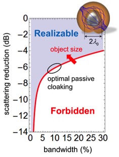
The researchers have prepared a diagram illustrating their work,

The graph shows the trade-off between how much an object can be made transparent (scattering reduction; vertical axis) and the color span (bandwidth; horizontal axis) over which this phenomenon can be achieved. Courtesy: University of Texas at Austin

The graph shows the trade-off between how much an object can be made transparent (scattering reduction; vertical axis) and the color span (bandwidth; horizontal axis) over which this phenomenon can be achieved. Courtesy: University of Texas at Austin

Here’s a link to and a citation for the paper,

Invisibility exposed: physical bounds on passive cloaking by Francesco Monticone and Andrea Alù. Optica Vol. 3, Issue 7, pp. 718-724 (2016) •doi: 10.1364/OPTICA.3.000718

This paper is open access.

Origami and our pop-up future

They should have declared Jan. 25, 2016 ‘L. Mahadevan Day’ at Harvard University. The researcher was listed as an author on two major papers. I covered the first piece of research, 4D printed hydrogels, in this Jan. 26, 2016 posting. Now for Mahadevan’s other work, from a Jan. 27, 2016 news item on Nanotechnology Now,

What if you could make any object out of a flat sheet of paper?

That future is on the horizon thanks to new research by L. Mahadevan, the Lola England de Valpine Professor of Applied Mathematics, Organismic and Evolutionary Biology, and Physics at the Harvard John A. Paulson School of Engineering and Applied Sciences (SEAS). He is also a core faculty member of the Wyss Institute for Biologically Inspired Engineering, and member of the Kavli Institute for Bionano Science and Technology, at Harvard University.

Mahadevan and his team have characterized a fundamental origami fold, or tessellation, that could be used as a building block to create almost any three-dimensional shape, from nanostructures to buildings. …

A Jan. 26, 2016 Harvard University news release by Leah Burrows, which originated the news item, provides more detail about the specific fold the team has been investigating,

The folding pattern, known as the Miura-ori, is a periodic way to tile the plane using the simplest mountain-valley fold in origami. It was used as a decorative item in clothing at least as long ago as the 15th century. A folded Miura can be packed into a flat, compact shape and unfolded in one continuous motion, making it ideal for packing rigid structures like solar panels.  It also occurs in nature in a variety of situations, such as in insect wings and certain leaves.

“Could this simple folding pattern serve as a template for more complicated shapes, such as saddles, spheres, cylinders, and helices?” asked Mahadevan.

“We found an incredible amount of flexibility hidden inside the geometry of the Miura-ori,” said Levi Dudte, graduate student in the Mahadevan lab and first author of the paper. “As it turns out, this fold is capable of creating many more shapes than we imagined.”

Think surgical stents that can be packed flat and pop-up into three-dimensional structures once inside the body or dining room tables that can lean flat against the wall until they are ready to be used.

“The collapsibility, transportability and deployability of Miura-ori folded objects makes it a potentially attractive design for everything from space-bound payloads to small-space living to laparoscopic surgery and soft robotics,” said Dudte.

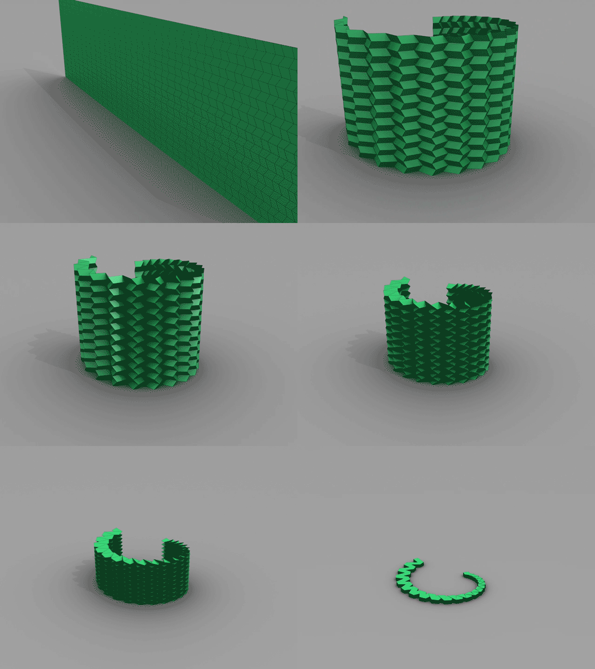
Here’s a .gif demonstrating the fold,

This spiral folds rigidly from flat pattern through the target surface and onto the flat-folded plane (Image courtesy of Mahadevan Lab) Harvard University

This spiral folds rigidly from flat pattern through the target surface and onto the flat-folded plane (Image courtesy of Mahadevan Lab) Harvard University

The news release offers some details about the research,

To explore the potential of the tessellation, the team developed an algorithm that can create certain shapes using the Miura-ori fold, repeated with small variations. Given the specifications of the target shape, the program lays out the folds needed to create the design, which can then be laser printed for folding.

The program takes into account several factors, including the stiffness of the folded material and the trade-off between the accuracy of the pattern and the effort associated with creating finer folds – an important characterization because, as of now, these shapes are all folded by hand.

“Essentially, we would like to be able to tailor any shape by using an appropriate folding pattern,” said Mahadevan. “Starting with the basic mountain-valley fold, our algorithm determines how to vary it by gently tweaking it from one location to the other to make a vase, a hat, a saddle, or to stitch them together to make more and more complex structures.”

“This is a step in the direction of being able to solve the inverse problem – given a functional shape, how can we design the folds on a sheet to achieve it,” Dudte said.

“The really exciting thing about this fold is it is completely scalable,” said Mahadevan. “You can do this with graphene, which is one atom thick, or you can do it on the architectural scale.”

Co-authors on the study include Etienne Vouga, currently at the University of Texas at Austin, and Tomohiro Tachi from the University of Tokyo. …

Here’s a link to and a citation for the paper,

Programming curvature using origami tessellations by Levi H. Dudte, Etienne Vouga, Tomohiro Tachi, & L. Mahadevan. Nature Materials (2016) doi:10.1038/nmat4540 Published online 25 January 2016

This paper is behind a paywall.

Nanotechnology-enabled flame retardant coating

This is a pretty remarkable demonstration made more so when you find out the flame retardant is naturally derived and nontoxic. From an Oct. 5, 2015 news item on Nanowerk,

Inspired by a naturally occurring material found in marine mussels, researchers at The University of Texas at Austin have created a new flame retardant to replace commercial additives that are often toxic and can accumulate over time in the environment and living animals, including humans.

An Oct. 5, 2015 University of Texas news release, which originated the news item, describes the situation with regard to standard flame retardants and what makes this new flame retardant technology so compelling,

Flame retardants are added to foams found in mattresses, sofas, car upholstery and many other consumer products. Once incorporated into foam, these chemicals can migrate out of the products over time, releasing toxic substances into the air and environment. Throughout the United States, there is pressure on state legislatures to ban flame retardants, especially those containing brominated compounds (BRFs), a mix of human-made chemicals thought to pose a risk to public health.

A team led by Cockrell School of Engineering associate professor Christopher Ellison found that a synthetic coating of polydopamine — derived from the natural compound dopamine — can be used as a highly effective, water-applied flame retardant for polyurethane foam. Dopamine is a chemical compound found in humans and animals that helps in the transmission of signals in the brain and other vital areas. The researchers believe their dopamine-based nanocoating could be used in lieu of conventional flame retardants.

“Since polydopamine is natural and already present in animals, this question of toxicity immediately goes away,” Ellison said. “We believe polydopamine could cheaply and easily replace the flame retardants found in many of the products that we use every day, making these products safer for both children and adults.”

Using far less polydopamine by weight than typical of conventional flame retardant additives, the UT Austin team found that the polydopamine coating on foams leads to a 67 percent reduction in peak heat release rate, a measure of fire intensity and imminent danger to building occupants or firefighters. The polydopamine flame retardant’s ability to reduce the fire’s intensity is about 20 percent better than existing flame retardants commonly used today.

Researchers have studied the use of synthetic polydopamaine for a number of health-related applications, including cancer drug delivery and implantable biomedical devices. However, the UT Austin team is thought to be one of the first to pursue the use of polydopamine as a flame retardant. To the research team’s surprise, they did not have to change the structure of the polydopamine from its natural form to use it as a flame retardant. The polydopamine was coated onto the interior and exterior surfaces of the polyurethane foam by simply dipping it into a water solution of dopamine for several days.

Ellison said he and his team were drawn to polydopamine because of its ability to adhere to surfaces as demonstrated by marine mussels who use the compound to stick to virtually any surface, including Teflon, the material used in nonstick cookware. Polydopamine also contains a dihydroxy-ring structure linked with an amine group that can be used to scavenge or remove free radicals. Free radicals are produced during the fire cycle as a polymer degrades, and their removal is critical to stopping the fire from continuing to spread. Polydopamine also produces a protective coating called char, which blocks fire’s access to its fuel source — the polymer. The synergistic combination of both these processes makes polydopamine an attractive and powerful flame retardant.

Ellison and his team are now testing to see whether they can shorten the nanocoating treatment process or develop a more convenient application process.

“We believe this alternative to flame retardants can prove very useful to removing potential hazards from products that children and adults use every day,” Ellison said. “We weren’t expecting to find a flame retardant in nature, but it was a serendipitous discovery.”

Here’s a link to and a citation for the paper,

Bioinspired Catecholic Flame Retardant Nanocoating for Flexible Polyurethane Foams by Joon Hee Cho, Vivek Vasagar, Kadhiravan Shanmuganathan, Amanda R. Jones, Sergei Nazarenko, and Christopher J. Ellison. Chem. Mater., 2015, 27 (19), pp 6784–6790 DOI: 10.1021/acs.chemmater.5b03013
Publication Date (Web): September 9, 2015
Copyright © 2015 American Chemical Society

This paper is behind a paywall. It should be noted that researchers from the University of Southern Mississippi and the Council of Scientific & Industrial Research (CSIR)-National Chemical Laboratory in Pune, India were also involved in this work.

An easier and cheaper way to make: wearable and disposable medical tattoolike patches

A Sept. 29, 2015 news item on ScienceDaily features an electronic health patch that’s cheaper and easier to make,

A team of researchers has invented a method for producing inexpensive and high-performing wearable patches that can continuously monitor the body’s vital signs for human health and performance tracking. The researchers believe their new method is compatible with roll-to-roll manufacturing.

The researchers have provided a photograph of a prototype patch,

Assitant professor Nanshu Lu and her team have developed a faster, inexpensive method for making epidermal electronics. Cockrell School of Engineering

Assitant professor Nanshu Lu and her team have developed a faster, inexpensive method for making epidermal electronics. Cockrell School of Engineering

A University of Texas at Austin Sept. 29, 2015 news release (also on EurekAlert), which originated the news item, provides more details,

Led by Assistant Professor Nanshu Lu, the team’s manufacturing method aims to construct disposable tattoo-like health monitoring patches for the mass production of epidermal electronics, a popular technology that Lu helped develop in 2011.

The team’s breakthrough is a repeatable “cut-and-paste” method that cuts manufacturing time from several days to only 20 minutes. The researchers believe their new method is compatible with roll-to-roll manufacturing — an existing method for creating devices in bulk using a roll of flexible plastic and a processing machine.

Reliable, ultrathin wearable electronic devices that stick to the skin like a temporary tattoo are a relatively new innovation. These devices have the ability to pick up and transmit the human body’s vital signals, tracking heart rate, hydration level, muscle movement, temperature and brain activity.

Although it is a promising invention, a lengthy, tedious and costly production process has until now hampered these wearables’ potential.

“One of the most attractive aspects of epidermal electronics is their ability to be disposable,” Lu said. “If you can make them inexpensively, say for $1, then more people will be able to use them more frequently. This will open the door for a number of mobile medical applications and beyond.”

The UT Austin method is the first dry and portable process for producing these electronics, which, unlike the current method, does not require a clean room, wafers and other expensive resources and equipment. Instead, the technique relies on freeform manufacturing, which is similar in scope to 3-D printing but different in that material is removed instead of added.

The two-step process starts with inexpensive, pre-fabricated, industrial-quality metal deposited on polymer sheets. First, an electronic mechanical cutter is used to form patterns on the metal-polymer sheets. Second, after removing excessive areas, the electronics are printed onto any polymer adhesives, including temporary tattoo films. The cutter is programmable so the size of the patch and pattern can be easily customized.

Deji Akinwande, an associate professor and materials expert in the Cockrell School, believes Lu’s method can be transferred to roll-to-roll manufacturing.

“These initial prototype patches can be adapted to roll-to-roll manufacturing that can reduce the cost significantly for mass production,” Akinwande said. “In this light, Lu’s invention represents a major advancement for the mobile health industry.”

After producing the cut-and-pasted patches, the researchers tested them as part of their study. In each test, the researchers’ newly fabricated patches picked up body signals that were stronger than those taken by existing medical devices, including an ECG/EKG, a tool used to assess the electrical and muscular function of the heart. The team also found that their patch conforms almost perfectly to the skin, minimizing motion-induced false signals or errors.

The UT Austin wearable patches are so sensitive that Lu and her team can envision humans wearing the patches to more easily maneuver a prosthetic hand or limb using muscle signals. For now, Lu said, “We are trying to add more types of sensors including blood pressure and oxygen saturation monitors to the low-cost patch.”

Here’s a link to and a citation for the paper,

“Cut-and-Paste” Manufacture of Multiparametric Epidermal Sensor Systems by Shixuan Yang, Ying-Chen Chen, Luke Nicolini, Praveenkumar Pasupathy, Jacob Sacks, Su Becky, Russell Yang, Sanchez Daniel, Yao-Feng Chang, Pulin Wang, David Schnyer, Dean Neikirk, and Nanshu Lu. Advanced Materials DOI: 10.1002/adma.201502386 First published: 23 September 2015

This paper is behind a paywall.

$81M for US National Nanotechnology Coordinated Infrastructure (NNCI)

Academics, small business, and industry researchers are the big winners in a US National Science Foundation bonanza according to a Sept. 16, 2015 news item on Nanowerk,

To advance research in nanoscale science, engineering and technology, the National Science Foundation (NSF) will provide a total of $81 million over five years to support 16 sites and a coordinating office as part of a new National Nanotechnology Coordinated Infrastructure (NNCI).

The NNCI sites will provide researchers from academia, government, and companies large and small with access to university user facilities with leading-edge fabrication and characterization tools, instrumentation, and expertise within all disciplines of nanoscale science, engineering and technology.

A Sept. 16, 2015 NSF news release provides a brief history of US nanotechnology infrastructures and describes this latest effort in slightly more detail (Note: Links have been removed),

The NNCI framework builds on the National Nanotechnology Infrastructure Network (NNIN), which enabled major discoveries, innovations, and contributions to education and commerce for more than 10 years.

“NSF’s long-standing investments in nanotechnology infrastructure have helped the research community to make great progress by making research facilities available,” said Pramod Khargonekar, assistant director for engineering. “NNCI will serve as a nationwide backbone for nanoscale research, which will lead to continuing innovations and economic and societal benefits.”

The awards are up to five years and range from $500,000 to $1.6 million each per year. Nine of the sites have at least one regional partner institution. These 16 sites are located in 15 states and involve 27 universities across the nation.

Through a fiscal year 2016 competition, one of the newly awarded sites will be chosen to coordinate the facilities. This coordinating office will enhance the sites’ impact as a national nanotechnology infrastructure and establish a web portal to link the individual facilities’ websites to provide a unified entry point to the user community of overall capabilities, tools and instrumentation. The office will also help to coordinate and disseminate best practices for national-level education and outreach programs across sites.

New NNCI awards:

Mid-Atlantic Nanotechnology Hub for Research, Education and Innovation, University of Pennsylvania with partner Community College of Philadelphia, principal investigator (PI): Mark Allen
Texas Nanofabrication Facility, University of Texas at Austin, PI: Sanjay Banerjee

Northwest Nanotechnology Infrastructure, University of Washington with partner Oregon State University, PI: Karl Bohringer

Southeastern Nanotechnology Infrastructure Corridor, Georgia Institute of Technology with partners North Carolina A&T State University and University of North Carolina-Greensboro, PI: Oliver Brand

Midwest Nano Infrastructure Corridor, University of  Minnesota Twin Cities with partner North Dakota State University, PI: Stephen Campbell

Montana Nanotechnology Facility, Montana State University with partner Carlton College, PI: David Dickensheets
Soft and Hybrid Nanotechnology Experimental Resource,

Northwestern University with partner University of Chicago, PI: Vinayak Dravid

The Virginia Tech National Center for Earth and Environmental Nanotechnology Infrastructure, Virginia Polytechnic Institute and State University, PI: Michael Hochella

North Carolina Research Triangle Nanotechnology Network, North Carolina State University with partners Duke University and University of North Carolina-Chapel Hill, PI: Jacob Jones

San Diego Nanotechnology Infrastructure, University of California, San Diego, PI: Yu-Hwa Lo

Stanford Site, Stanford University, PI: Kathryn Moler

Cornell Nanoscale Science and Technology Facility, Cornell University, PI: Daniel Ralph

Nebraska Nanoscale Facility, University of Nebraska-Lincoln, PI: David Sellmyer

Nanotechnology Collaborative Infrastructure Southwest, Arizona State University with partners Maricopa County Community College District and Science Foundation Arizona, PI: Trevor Thornton

The Kentucky Multi-scale Manufacturing and Nano Integration Node, University of Louisville with partner University of Kentucky, PI: Kevin Walsh

The Center for Nanoscale Systems at Harvard University, Harvard University, PI: Robert Westervelt

The universities are trumpeting this latest nanotechnology funding,

NSF-funded network set to help businesses, educators pursue nanotechnology innovation (North Carolina State University, Duke University, and University of North Carolina at Chapel Hill)

Nanotech expertise earns Virginia Tech a spot in National Science Foundation network

ASU [Arizona State University] chosen to lead national nanotechnology site

UChicago, Northwestern awarded $5 million nanotechnology infrastructure grant

That is a lot of excitement.

Does the universe have a heartbeat?

It may be a bit fanciful to suggest the universe has a heartbeat but if University of Warwick (UK) researchers can state that dying stars have ‘irregular heartbeats’ then why can’t the universe have a heartbeat of sorts? Getting back to the University of Warwick, their August 26, 2015 press release (also on EurekAlert) has this to say,

Some dying stars suffer from ‘irregular heartbeats’, research led by astronomers at the University of Warwick has discovered.

The research confirms rapid brightening events in otherwise normal pulsating white dwarfs, which are stars in the final stage of their life cycles.

In addition to the regular rhythm from pulsations they expected on the white dwarf PG1149+057, which cause the star to get a few percent brighter and fainter every few minutes, the researchers also observed something completely unexpected every few days: arrhythmic, massive outbursts, which broke the star’s regular pulse and significantly heated up its surface for many hours.

The discovery was made possible by using the planet-hunting spacecraft Kepler, which stares unblinkingly at a small patch of sky, uninterrupted by clouds or sunrises.

Led by Dr JJ Hermes of the University of Warwick’s Astrophysics Group, the astronomers targeted the Kepler spacecraft on a specific star in the constellation Virgo, PG1149+057, which is roughly 120 light years from Earth.

Dr Hermes explains:

“We have essentially found rogue waves in a pulsating star, akin to ‘irregular heartbeats’. These were truly a surprise to see: we have been watching pulsating white dwarfs for more than 50 years now from the ground, and only by being able to stare uninterrupted for months from space have we been able to catch these events.”

The star with the irregular beat, PG1149+057, is a pulsating white dwarf, which is the burnt-out core of an evolved star, an extremely dense star which is almost entirely made up of carbon and oxygen. Our Sun will eventually become a white dwarf in more than six billion years, after it runs out of its nuclear fuel.

White dwarfs have been known to pulsate for decades, and some are exceptional clocks, with pulsations that have kept nearly perfect time for more than 40 years. Pulsations are believed to be a naturally occurring stage when a white dwarf reaches the right temperature to generate a mix of partially ionized hydrogen atoms at its surface.

That mix of excited atoms can store up and then release energy, causing the star to resonate with pulsations characteristically every few minutes. Astronomers can use the regular periods of these pulsations just like seismologists use earthquakes on Earth, to see below the surface of the star into its exotic interior. This was why astronomers targeted PG1149+057 with Kepler, hoping to learn more about its dense core. In the process, they caught a new glimpse at these unexpected outbursts.

“These are highly energetic events, which can raise the star’s overall brightness by more than 15% and its overall temperature by more than 750 degrees in a matter of an hour,” said Dr Hermes. “For context, the Sun will only increase in overall brightness by about 1% over the next 100 million years.”

Interestingly, this is not the only white dwarf to show an irregular pulse. Recently, the Kepler spacecraft witnessed the first example of these strange outbursts while studying another white dwarf, KIC 4552982, which was observed from space for more than 2.5 years.

There is a narrow range of surface temperatures where pulsations can be excited in white dwarfs, and so far irregularities have only been seen in the coolest of those that pulsate. Thus, these irregular outbursts may not be just an oddity; they have the potential to change the way astronomers understand how pulsations, the regular heartbeats, ultimately cease in white dwarfs.

“The theory of stellar pulsations has long failed to explain why pulsations in white dwarfs stop at the temperature we observe them to,” argues Keaton Bell of the University of Texas at Austin, who analysed the first pulsating white dwarf to show an irregular heartbeat, KIC 4552982. “That both stars exhibiting this new outburst phenomenon are right at the temperature where pulsations shut down suggests that the outbursts could be the key to revealing the missing physics in our pulsation theory.”

Astronomers are still trying to settle on an explanation for these never-before-seen outbursts. Given the similarity between the first two stars to show this behaviour, they suspect it might have to do with how the pulsation waves interact with themselves, perhaps via a resonance.

“Ultimately, this may be a new type of nonlinear behaviour that is triggered when the amplitude of a pulsation passes a certain threshold, perhaps similar to rogue waves on the open seas here on Earth, which are massive, spontaneous waves that can be many times larger than average surface waves,” said Dr Hermes. “Still, this is a fresh discovery from observations, and there may be more to these irregular stellar heartbeats than we can imagine yet.”

Here’s a link to and a citation for the paper,

A Second Case of Outbursts in a Pulsating White Dwarf Observed by Kepler by J. J. Hermes, M. H. Montgomery, Keaton J. Bell, P. Chote, B. T. Gänsicke, Steven D. Kawaler, J. C. Clemens, Bart H. Dunlap, D. E. Winget, and D. J. Armstrong.
2015 ApJ 810 L5 (The Astrophysical Journal Letters Volume 810 Number 1). doi:10.1088/2041-8205/810/1/L5
Published 24 August 2015.

© 2015. The American Astronomical Society. All rights reserved.

This paper is behind a paywall but there is an earlier open access version available at arXiv.org,

A second case of outbursts in a pulsating white dwarf observed by Kepler by J. J. Hermes, M. H. Montgomery, Keaton J. Bell, P. Chote, B. T. Gaensicke, Steven D. Kawaler, J. C. Clemens, B. H. Dunlap, D. E. Winget, D. J. Armstrong.  arXiv.org > astro-ph > arXiv:1507.06319

In an attempt to find some live heart beats to illustrate this piece, I found this video from Wake Forest University’s body-on-a-chip program,

The video was released in an April 14, 2015 article by Joe Bargmann for Popular Mechanics,

A groundbreaking program has converted human skin cells into a network of functioning heart cells, and also fused them with lab-grown liver cells using a specialized 3D printer. Researchers at the Wake Forest Baptist Medical Center’s Institute for Regenerative Medicine provided Popular Mechanics with both still and moving images of the cells for a fascinating first look.

“The heart organoid beats because it contains specialized cardiac cells and because those cells are receiving the correct environmental cues,” says Ivy Mead, a Wake Forest graduate student and member of the research team. “We give them a special medium and keep them at the same temperature as the human body, and that makes them beat. We can also stimulate the miniature organ with electrical or chemical cues to alter the beating patterns. Also, when we grow them in three-dimensions it allows for them to interact with each other more easily, as they would in the human body.”

If you’re interested in body-on-a-chip projects, I have several stories here (suggestion: use body-on-a-chip as your search term in the blog search engine) and I encourage you to read Bargmann’s story in its entirety (the video no longer seems to be embedded there).

One final comment, there seems to be some interest in relating large systems to smaller ones. For example, humans and other animals along with white dwarf stars have heartbeats (as in this story) and patterns in a gold nanoparticle of 133 atoms resemble the Milky Way (my April 14, 2015 posting titled: Nature’s patterns reflected in gold nanoparticles).

Smart windows from Texas (US)

I’ve been waiting for ‘smart’ windows and/or self-cleaning windows since 2008. While this research on ‘smart’ windows at the University of Texas at Austin looks promising I suspect it will be years before these things are in the marketplace. A July 22, 2015 news item on Nanotechnology Now announces the latest research,

Researchers in the Cockrell School of Engineering at The University of Texas at Austin are one step closer to delivering smart windows with a new level of energy efficiency, engineering materials that allow windows to reveal light without transferring heat and, conversely, to block light while allowing heat transmission, as described in two new research papers.

By allowing indoor occupants to more precisely control the energy and sunlight passing through a window, the new materials could significantly reduce costs for heating and cooling buildings.

In 2013, chemical engineering professor Delia Milliron and her team became the first to develop dual-band electrochromic materials that blend two materials with distinct optical properties for selective control of visible and heat-producing near-infrared light (NIR). In a 2013 issue of Nature, Milliron’s research group demonstrated how, using a small jolt of electricity, a nanocrystal material could be switched back and forth, enabling independent control of light and energy.

A July 23, 2015 University of Texas at Austin news release, which originated the news item, provides more details about the research which has spawned two recently published papers,

The team now has engineered two new advancements in electrochromic materials — a highly selective cool mode and a warm mode — not thought possible several years ago.

The cool mode material is a major step toward a commercialized product because it enables control of 90 percent of NIR and 80 percent of the visible light from the sun and takes only minutes to switch between modes. The previously reported material could require hours.

To achieve this high performance, Milliron and a team, including Cockrell School postdoctoral researcher Jongwook Kim and collaborator Brett Helms of the Lawrence Berkeley National Lab, developed a new nanostructured architecture for electrochromic materials that allows for a cool mode to block near-infrared light while allowing the visible light to shine through. This could help reduce energy costs for cooling buildings and homes during the summer. The researchers reported the new architecture in Nano Letters on July 20.

“We believe our new architected nanocomposite could be seen as a model material, establishing the ideal design for a dual-band electrochromic material,” Milliron said. “This material could be ideal for application as a smart electrochromic window for buildings.”

In the paper, the team demonstrates how the new material can strongly and selectively modulate visible light and NIR by applying a small voltage.

To optimize the performance of electrochromics for practical use, the team organized the two components of the composite material to create a porous interpenetrating network. The framework architecture provides channels for transport of electronic and ionic change. This organization enables substantially faster switching between modes.
Smart Window

The researchers are now working to produce a similarly structured nanocomposite material by simple methods, suitable for low-cost manufacturing.

In a second research paper, Milliron and her team, including Cockrell School graduate student Clayton Dahlman, have reported a proof-of-concept demonstrating how they can achieve optical control properties in windows from a well-crafted, single-component film. The concept includes a simple coating that creates a new warm mode, in which visible light can be blocked, while near-infrared light can enter. This new setting could be most useful on a sunny winter day, when an occupant would want infrared radiation to pass into a building for warmth, but the glare from sunlight to be reduced.

In this paper, published in the Journal of the American Chemical Society, Milliron proved that a coating containing a single component ­— doped titania nanocrystals — could demonstrate dynamic control over the transmittance of solar radiation. Because of two distinct charging mechanisms found at different applied voltages, this material can selectively block visible or infrared radiation.

“These two advancements show that sophisticated dynamic control of sunlight is possible,” Milliron said. “We believe our deliberately crafted nanocrystal-based materials could meet the performance and cost targets needed to progress toward commercialization of smart windows.”

Interestingly, the news release includes this statement,

The University of Texas at Austin is committed to transparency and disclosure of all potential conflicts of interest. The lead UT investigator involved with this project, Delia Milliron, is the chief scientific officer and owns an equity position in Heliotrope Technologies, an early-stage company developing new materials and manufacturing processes for electrochromic devices with an emphasis on energy-saving smart windows. Milliron is associated with patents at Lawrence Berkeley National Laboratory licensed to Heliotrope Technologies. Collaborator Brett Helms serves on the scientific advisory board of Heliotrope and owns equity in the company.

Here are links to and citations for the two papers,

Nanocomposite Architecture for Rapid, Spectrally-Selective Electrochromic Modulation of Solar Transmittance by Jongwook Kim, Gary K. Ong, Yang Wang, Gabriel LeBlanc, Teresa E. Williams, Tracy M. Mattox, Brett A. Helms, and Delia J. Milliron. Nano Lett., Article ASAP DOI: 10.1021/acs.nanolett.5b02197 Publication Date (Web): July 20, 2015

Copyright © 2015 American Chemical Society

Spectroelectrochemical Signatures of Capacitive Charging and Ion Insertion in Doped Anatase Titania Nanocrystals by Clayton J. Dahlman, Yizheng Tan, Matthew A. Marcus, and Delia J. Milliron. J. Am. Chem. Soc., 2015, 137 (28), pp 9160–9166 DOI: 10.1021/jacs.5b04933 Publication Date (Web): July 8, 2015

Copyright © 2015 American Chemical Society

These papers are behind paywalls.

TRIUMF accelerator used by US researchers to visualize properties of nanoscale materials

The US researchers are at the University of California at Los Angeles (UCLA) and while it’s not explicitly stated I’m assuming the accelerator they mention at TRIUMF (Canada’s national laboratory for particle and nuclear physics) has something special as there are accelerators in California and other parts of the US.

A July 15, 2015 news item on Nanotechnology Now announces the latest on visualizing the properties of nanoscale materials,

Scientists trying to improve the semiconductors that power our electronic devices have focused on a technology called spintronics as one especially promising area of research. Unlike conventional devices that use electrons’ charge to create power, spintronic devices use electrons’ spin. The technology is already used in computer hard drives and many other applications — and scientists believe it could eventually be used for quantum computers, a new generation of machines that use quantum mechanics to solve complex problems with extraordinary speed.

A July 15, 2015 UCLA news release, which originated the news item, expands on the theme and briefly mentions TRIUMF’s accelerator (Note: A link has been removed),

Emerging research has shown that one key to greatly improving performance in spintronics could be a class of materials called topological insulators. Unlike ordinary materials that are either insulators or conductors, topological insulators function as both simultaneously — on the inside, they are insulators but on their exteriors, they conduct electricity.

But topological insulators have certain defects that have so far limited their use in practical applications, and because they are so tiny, scientists have so far been unable to fully understand how the defects impact their functionality.

The UCLA researchers have overcome that challenge with a new method to visualize topological insulators at the nanoscale. An article highlighting the research, which was which led by Louis Bouchard, assistant professor of chemistry and biochemistry, and Dimitrios Koumoulis, a UCLA postdoctoral scholar, was published online in the Proceedings of the National Academy of Sciences.

The new method is the first use of beta‑detected nuclear magnetic resonance to study the effects of these defects on the properties of topological insulators.

The technique involves aiming a highly focused stream of ions at the topological insulator. To generate that beam of ions, the researchers used a large particle accelerator called a cyclotron, which accelerates protons through a spiral path inside the machine and forces them to collide with a target made of the chemical element tantalum. This collision produces lithium-8 atoms, which are ionized and slowed down to a desired energy level before they are implanted in the topological insulators.

In beta‑detected nuclear magnetic resonance, ions (in this case, the ionized lithium-8 atoms) of various energies are implanted in the material of interest (the topological insulator) to generate signals from the material’s layers of interest.

Bouchard said the method is particularly well suited for probing regions near the surfaces and interfaces of different materials.

In the UCLA research, the high sensitivity of the beta‑detected nuclear magnetic resonance technique and its ability to probe materials allowed the scientists to “see” the impacts of the defects in the topological insulators by viewing the electronic and magnetic properties beneath the surface of the material.

The researchers used the large TRIUMF cyclotron in Vancouver, British Columbia.

According to the UCLA news release, there were also researchers from the University of British Columbia, the University of Texas at Austin and Northwestern University *were* involved with the work.

Here’s a link to and a citation for the paper,

Nanoscale β-nuclear magnetic resonance depth imaging of topological insulators by Dimitrios Koumoulis, Gerald D. Morris, Liang He, Xufeng Kou, Danny King, Dong Wang, Masrur D. Hossain, Kang L. Wang, Gregory A. Fiete, Mercouri G. Kanatzidis, and Louis-S. Bouchard. PNAS July 14, 2015 vol. 112 no. 28 doi: 10.1073/pnas.1502330112

This paper is behind a paywall.

*’were’ added Jan. 20, 2016.

Battery-powered invisibiity cloak

You’d never guess it from the title of their paper but researchers at the University of Texas at Austin have conceptualized and designed a battery-operated invisibility cloak, according to a Dec. 18, 2013 news item on Nanowerk,

Researchers at The University of Texas at Austin have proposed the first design of a cloaking device that uses an external source of energy to significantly broaden its bandwidth of operation.

Andrea Alù, associate professor in the Department of Electrical and Computer Engineering at the Cockrell School of Engineering, and his team have proposed a design for an active cloak that draws energy from a battery, allowing objects to become undetectable to radio sensors over a greater range of frequencies.

The Dec. 18, 2013 University of Texas at Austin news release (also on EurekAlert), which originated the news item, describes the current state of cloaking technology,

Cloaks have so far been realized with so-called passive technology, which means that they are not designed to draw energy from an external source. They are typically based on metamaterials (advanced artificial materials) or metasurfaces (a flexible, ultrathin metamaterial) that can suppress the scattering of light that bounces off an object, making an object less visible. When the scattered fields from the cloak and the object interfere, they cancel each other out, and the overall effect is transparency to radio-wave detectors. They can suppress 100 times or more the detectability at specific design frequencies. Although the proposed design works for radio waves, active cloaks could one day be designed to make detection by the human eye more difficult.

“Many cloaking designs are good at suppressing the visibility under certain conditions, but they are inherently limited to work for specific colors of light or specific frequencies of operation,” said Alù, David & Doris Lybarger Endowed Faculty Fellow in the Department of Electrical and Computer Engineering. In this paper, on the contrary, “we prove that cloaks can become broadband, pushing this technology far beyond current limits of passive cloaks. I believe that our design helps us understand the fundamental challenges of suppressing the scattering of various objects at multiple wavelengths and shows a realistic path to overcome them.”

The news release details the new battery-powered design,

The proposed active cloak uses a battery, circuits and amplifiers to boost signals, which makes possible the reduction of scattering over a greater range of frequencies. This design, which covers a very broad frequency range, will provide the most broadband and robust performance of a cloak to date. Additionally, the proposed active technology can be thinner and less conspicuous than conventional cloaks.

In a related paper, published in Physical Review X in October, Alù and his graduate student Francesco Monticone proved that existing passive cloaking solutions are fundamentally limited in the bandwidth of operation and cannot provide broadband cloaking. When viewed at certain frequencies, passively cloaked objects may indeed become transparent, but if illuminated with white light, which is composed of many colors, they are bound to become more visible with the cloak than without. The October paper proves that all available cloaking techniques based on passive cloaks are constrained by Foster’s theorem, which limits their overall ability to cancel the scattering across a broad frequency spectrum.

In contrast, an active cloak based on active metasurfaces, such as the one designed by Alù’s team, can break Foster’s theorem limitations. The team started with a passive metasurface made from an array of metal square patches and loaded it with properly positioned operational amplifiers that use the energy drawn from a battery to broaden the bandwidth.

“In our case, by introducing these suitable amplifiers along the cloaking surface, we can break the fundamental limits of passive cloaks and realize a ‘non-Foster’ surface reactance that decreases, rather than increases, with frequency, significantly broadening the bandwidth of operation,” Alù said.

The researchers are continuing to work both on the theory and design behind their non-Foster active cloak, and they plan to build a prototype.

Alù and his team are working to use active cloaks to improve wireless communications by suppressing the disturbance that neighboring antennas produce on transmitting and receiving antennas. They have also proposed to use these cloaks to improve biomedical sensing, near-field imaging and energy harvesting devices.

Here’s a link to and a citation for the team’s paper about active cloaking,

Broadening the Cloaking Bandwidth with Non-Foster Metasurfaces by Pai-Yen Chen, Christos Argyropoulos, and Andrea Alù. Phys. Rev. Lett. 111, 233001 (2013) [5 pages] DOI: 10.1103/PhysRevLett.111.233001

This paper is behind a paywall.

Here’s a link to and a citation for the related and previously published paper (authors: Alù and Monticone),

Do Cloaked Objects Really Scatter Less? by Francesco Monticone and Andrea Alù. Phys. Rev. X 3, 041005 (2013) [10 pages] DOI: 10.1103/PhysRevX.3.041005

The authors have included both an abstract and a popular summary. I’ve excerpted the popular summary,

From ancient times, humanity has been fascinated by the concept of invisibility, and recently, scientists have moved a step closer to bringing this idea to reality by exploiting engineered artificial materials, or metamaterials. Several recent studies have indeed shown that a properly tailored metamaterial cover can, in principle, render an object invisible when illuminated by an electromagnetic wave oscillating at the specific frequency of interest. Yet, experimental realizations and theoretical investigations have consistently shown that reducing the visibility of an object with a passive cloak in a specific window of the electromagnetic spectrum is generally accompanied by a drastic increase of its visibility in other frequency ranges. Making an object invisible to red light, for instance, may actually make it bright blue, increasing its overall visibility.

In this paper, we quantitatively assess the potentials and limitations of passive cloaks in terms of overall visibility, integrated over the entire frequency spectrum. Quite surprisingly, our results show that any linear, causal, and passive invisibility cloak, without special superconducting features, is deemed to increase the scattering and visibility of the original uncloaked object, when integrated over all frequencies. This result confirms that the most popular cloaking devices actually scatter more, not less, when considered over a sufficiently broad frequency range, allowing easy detection using, e.g., pulsed excitation.

Our general theorem holds a relevant exception if specific covers with a strong static diamagnetism are considered, and, based on this principle, we propose a technique to reduce the global scattering, as well as the local response around a frequency of interest, using diamagnetic and superconducting thin cloaking layers. More generally, our results provide a quantitative measure to compare the overall performance of different cloaking devices and generally assess their detectability. These findings may open important research directions in the quest for invisibility, not only in the electromagnetic domain but also for acoustic, mechanical, and matter waves.

This is an open access paper.