Imagine a box you plug into the wall that cleans your toxic air and pays you cash.
That’s essentially what Vanderbilt University researchers produced after discovering the blueprint for turning the carbon dioxide into carbon nanotubes with small diameters.
Carbon nanotubes are supermaterials that can be stronger than steel and more conductive than copper. The reason they’re not in every application from batteries to tires is that these amazing properties only show up in the tiniest nanotubes, which are extremely expensive. Not only did the Vanderbilt team show they can make these materials from carbon dioxide sucked from the air, but how to do this in a way that is much cheaper than any other method out there.
I’m not sure what ‘small’ means in this context. I’ve heard of long and short carbon nanotubes (CNTs) and also of single-walled, multi-walled, and double-walled CNTs. I wish there’d been an an explanation and measurements for ‘small diameter CNTs’. That nitpick aside, a May 23, 2018 Vanderbilt University news release by Heidi Hall adds a few more technical details,
These materials, which Assistant Professor of Mechanical Engineering Cary Pint calls “black gold,” could steer the conversation from the negative impact of emissions to how we can use them in future technology.
“One of the most exciting things about what we’ve done is use electrochemistry to pull apart carbon dioxide into elemental constituents of carbon and oxygen and stitch together, with nanometer precision, those carbon atoms into new forms of matter,” Pint said. “That opens the door to being able to generate really valuable products with carbon nanotubes.
“These could revolutionize the world.”
In a report published today in ACS [American Chemical Society] Applied Materials and Interfaces, Pint, interdisciplinary material science Ph.D. student Anna Douglas and their team describe how tiny nanoparticles 10,000 times smaller than a human hair can be produced from coatings on stainless steel surfaces. The key was making them small enough to be valuable.
“The cheapest carbon nanotubes on the market cost around $100-200 per kilogram,” Douglas said. “Our research advance demonstrates a pathway to synthesize carbon nanotubes better in quality than these materials with lower cost and using carbon dioxide captured from the air.”
But making small nanotubes is no small task. The research team showed that a process called Ostwald ripening — where the nanoparticles that grow the carbon nanotubes change in size to larger diameters — is a key contender against producing the infinitely more useful size. The team showed they could partially overcome this by tuning electrochemical parameters to minimize these pesky large nanoparticles.
Small diameter carbon nanotubes grown on a stainless steel surface. (Pint Lab/Vanderbilt University)
This core technology led Pint and Douglas to co-found SkyNano LLC, a company focused on building upon the science of this process to scale up and commercialize products from these materials.
“What we’ve learned is the science that opens the door to now build some of the most valuable materials in our world, such as diamonds and single-walled carbon nanotubes, from carbon dioxide that we capture from air through our process,” Pint said.
From time to time I check out the latest on attempts to shrink computer chips. In my July 11, 2014 posting I noted IBM’s announcement about developing a 7nm computer chip and later in my July 15, 2015 posting I noted IBM’s announcement of a working 7nm chip (from a July 9, 2015 IBM news release , “The breakthrough, accomplished in partnership with GLOBALFOUNDRIES and Samsung at SUNY Polytechnic Institute’s Colleges of Nanoscale Science and Engineering (SUNY Poly CNSE), could result in the ability to place more than 20 billion tiny switches — transistors — on the fingernail-sized chips that power everything from smartphones to spacecraft.”
I’m not sure what happened to the IBM/Global Foundries/Samsung partnership but Global Foundries recently announced that it will no longer be working on 7nm chips. From an August 27, 2018 Global Foundries news release,
GLOBALFOUNDRIES [GF] today announced an important step in its transformation, continuing the trajectory launched with the appointment of Tom Caulfield as CEO earlier this year. In line with the strategic direction Caulfield has articulated, GF is reshaping its technology portfolio to intensify its focus on delivering truly differentiated offerings for clients in high-growth markets.
GF is realigning its leading-edge FinFET roadmap to serve the next wave of clients that will adopt the technology in the coming years. The company will shift development resources to make its 14/12nm FinFET platform more relevant to these clients, delivering a range of innovative IP and features including RF, embedded memory, low power and more. To support this transition, GF is putting its 7nm FinFET program on hold indefinitely [emphasis mine] and restructuring its research and development teams to support its enhanced portfolio initiatives. This will require a workforce reduction, however a significant number of top technologists will be redeployed on 14/12nm FinFET derivatives and other differentiated offerings.
I tried to find a definition for FinFet but the reference to a MOSFET and in-gate transistors was too much incomprehensible information packed into a tight space, see the FinFET Wikipedia entry for more, if you dare.
Getting back to the 7nm chip issue, Samuel K. Moore (I don’t think he’s related to the Moore of Moore’s law) wrote an Aug. 28, 2018 posting on the Nanoclast blog (on the IEEE [Institute of Electronics and Electrical Engineers] website) which provides some insight (Note: Links have been removed),
In a major shift in strategy, GlobalFoundries is halting its development of next-generation chipmaking processes. It had planned to move to the so-called 7-nm node, then begin to use extreme-ultraviolet lithography (EUV) to make that process cheaper. From there, it planned to develop even more advanced lithography that would allow for 5- and 3-nanometer nodes. Despite having installed at least one EUV machine at its Fab 8 facility in Malta, N.Y., all those plans are now on indefinite hold, the company announced Monday.
The move leaves only three companies reaching for the highest rungs of the Moore’s Law ladder: Intel, Samsung, and TSMC.
It’s a huge turnabout for GlobalFoundries. …
GlobalFoundries rationale for the move is that there are not enough customers that need bleeding-edge 7-nm processes to make it profitable. “While the leading edge gets most of the headlines, fewer customers can afford the transition to 7 nm and finer geometries,” said Samuel Wang, research vice president at Gartner, in a GlobalFoundries press release.
“The vast majority of today’s fabless [emphasis mine] customers are looking to get more value out of each technology generation to leverage the substantial investments required to design into each technology node,” explained GlobalFoundries CEO Tom Caulfield in a press release. “Essentially, these nodes are transitioning to design platforms serving multiple waves of applications, giving each node greater longevity. This industry dynamic has resulted in fewer fabless clients designing into the outer limits of Moore’s Law. We are shifting our resources and focus by doubling down on our investments in differentiated technologies across our entire portfolio that are most relevant to our clients in growing market segments.”
(The dynamic Caulfield describes is something the U.S. Defense Advanced Research Agency is working to disrupt with its $1.5-billion Electronics Resurgence Initiative. Darpa’s [DARPA] partners are trying to collapse the cost of design and allow older process nodes to keep improving by using 3D technology.)
…
Fabless manufacturing is where the fabrication is outsourced and the manufacturing company of record is focused on other matters according to the Fabless manufacturing Wikipedia entry.
Roland Moore-Colyer (I don’t think he’s related to Moore of Moore’s law either) has written August 28, 2018 article for theinquirer.net which also explores this latest news from Global Foundries (Note: Links have been removed),
EVER PREPPED A SPREAD for a party to then have less than half the people you were expecting show up? That’s probably how GlobalFoundries [sic] feels at the moment.
The chip manufacturer, which was once part of AMD, had a fabrication process geared up for 7-nanometre chips which its customers – including AMD and Qualcomm – were expected to adopt.
But AMD has confirmed that it’s decided to move its 7nm GPU production to TSMC, and Intel is still stuck trying to make chips based on 10nm fabrication.
…
Arguably, this could mark a stymieing of innovation and cutting-edge designs for chips in the near future. But with processors like AMD’s Threadripper 2990WX overclocked to run at 6GHz across all its 32 cores, in the real-world PC fans have no need to worry about consumer chips running out of puff anytime soon. µ
That’s all folks.
Maybe that’s not all
Steve Blank in a Sept. 10, 2018 posting on the Nanoclast blog (on the IEEE [Institute of Electrical and Electronics Engineers] website) provides some provocative commentary on the Global Foundries announcement (Note: A link has been removed),
For most of our lives, the idea that computers and technology would get better, faster, and cheaper every year was as assured as the sun rising every morning. The story “GlobalFoundries Halts 7-nm Chip Development” doesn’t sound like the end of that era, but for you and anyone who uses an electronic device, it most certainly is.
Technology innovation is going to take a different direction.
…
This story just goes on and on
There was a new development according to a Sept. 12, 2018 posting on the Nanoclast blog by, again, Samuel K. Moore (Note Links have been removed),
At an event today [sept. 12, 2018], Apple executives said that the new iPhone Xs and Xs Max will contain the first smartphone processor to be made using 7 nm manufacturing technology, the most advanced process node. Huawei made the same claim, to less fanfare, late last month and it’s unclear who really deserves the accolades. If anybody does, it’s TSMC, which manufactures both chips.
TSMC went into volume production with 7-nm tech in April, and rival Samsung is moving toward commercial 7-nm production later this year or in early 2019. GlobalFoundries recently abandoned its attempts to develop a 7 nm process, reasoning that the multibillion-dollar investment would never pay for itself. And Intel announced delays in its move to its next manufacturing technology, which it calls a 10-nm node but which may be equivalent to others’ 7-nm technology.
…
There’s a certain ‘soap opera’ quality to this with all the twists and turns.
An April 18, 2018 news item on phys.org highlights an exciting graphene development at the Massachusetts Institute of Technology (MIT),
MIT engineers have developed a continuous manufacturing process that produces long strips of high-quality graphene.
The team’s results are the first demonstration of an industrial, scalable method for manufacturing high-quality graphene that is tailored for use in membranes that filter a variety of molecules, including salts, larger ions, proteins, or nanoparticles. Such membranes should be useful for desalination, biological separation, and other applications.
A new manufacturing process produces strips of graphene, at large scale, for use in membrane technologies and other applications. Image: Christine Daniloff, MIT
“For several years, researchers have thought of graphene as a potential route to ultrathin membranes,” says John Hart, associate professor of mechanical engineering and director of the Laboratory for Manufacturing and Productivity at MIT. “We believe this is the first study that has tailored the manufacturing of graphene toward membrane applications, which require the graphene to be seamless, cover the substrate fully, and be of high quality.”
Hart is the senior author on the paper, which appears online in the journal Applied Materials and Interfaces. The study includes first author Piran Kidambi, a former MIT postdoc who is now an assistant professor at Vanderbilt University; MIT graduate students Dhanushkodi Mariappan and Nicholas Dee; Sui Zhang of the National University of Singapore; Andrey Vyatskikh, a former student at the Skolkovo Institute of Science and Technology who is now at Caltech; and Rohit Karnik, an associate professor of mechanical engineering at MIT.
Growing graphene
For many researchers, graphene is ideal for use in filtration membranes. A single sheet of graphene resembles atomically thin chicken wire and is composed of carbon atoms joined in a pattern that makes the material extremely tough and impervious to even the smallest atom, helium.
Researchers, including Karnik’s group, have developed techniques to fabricate graphene membranes and precisely riddle them with tiny holes, or nanopores, the size of which can be tailored to filter out specific molecules. For the most part, scientists synthesize graphene through a process called chemical vapor deposition, in which they first heat a sample of copper foil and then deposit onto it a combination of carbon and other gases.
Graphene-based membranes have mostly been made in small batches in the laboratory, where researchers can carefully control the material’s growth conditions. However, Hart and his colleagues believe that if graphene membranes are ever to be used commercially they will have to be produced in large quantities, at high rates, and with reliable performance.
“We know that for industrialization, it would need to be a continuous process,” Hart says. “You would never be able to make enough by making just pieces. And membranes that are used commercially need to be fairly big – some so big that you would have to send a poster-wide sheet of foil into a furnace to make a membrane.”
A factory roll-out
The researchers set out to build an end-to-end, start-to-finish manufacturing process to make membrane-quality graphene.
The team’s setup combines a roll-to-roll approach – a common industrial approach for continuous processing of thin foils – with the common graphene-fabrication technique of chemical vapor deposition, to manufacture high-quality graphene in large quantities and at a high rate. The system consists of two spools, connected by a conveyor belt that runs through a small furnace. The first spool unfurls a long strip of copper foil, less than 1 centimeter wide. When it enters the furnace, the foil is fed through first one tube and then another, in a “split-zone” design.
While the foil rolls through the first tube, it heats up to a certain ideal temperature, at which point it is ready to roll through the second tube, where the scientists pump in a specified ratio of methane and hydrogen gas, which are deposited onto the heated foil to produce graphene.
“Graphene starts forming in little islands, and then those islands grow together to form a continuous sheet,” Hart says. “By the time it’s out of the oven, the graphene should be fully covering the foil in one layer, kind of like a continuous bed of pizza.”
As the graphene exits the furnace, it’s rolled onto the second spool. The researchers found that they were able to feed the foil continuously through the system, producing high-quality graphene at a rate of 5 centimers per minute. Their longest run lasted almost four hours, during which they produced about 10 meters of continuous graphene.
“If this were in a factory, it would be running 24-7,” Hart says. “You would have big spools of foil feeding through, like a printing press.”
Flexible design
Once the researchers produced graphene using their roll-to-roll method, they unwound the foil from the second spool and cut small samples out. They cast the samples with a polymer mesh, or support, using a method developed by scientists at Harvard University, and subsequently etched away the underlying copper.
“If you don’t support graphene adequately, it will just curl up on itself,” Kidambi says. “So you etch copper out from underneath and have graphene directly supported by a porous polymer – which is basically a membrane.”
The polymer covering contains holes that are larger than graphene’s pores, which Hart says act as microscopic “drumheads,” keeping the graphene sturdy and its tiny pores open.
The researchers performed diffusion tests with the graphene membranes, flowing a solution of water, salts, and other molecules across each membrane. They found that overall, the membranes were able to withstand the flow while filtering out molecules. Their performance was comparable to graphene membranes made using conventional, small-batch approaches.
The team also ran the process at different speeds, with different ratios of methane and hydrogen gas, and characterized the quality of the resulting graphene after each run. They drew up plots to show the relationship between graphene’s quality and the speed and gas ratios of the manufacturing process. Kidambi says that if other designers can build similar setups, they can use the team’s plots to identify the settings they would need to produce a certain quality of graphene.
“The system gives you a great degree of flexibility in terms of what you’d like to tune graphene for, all the way from electronic to membrane applications,” Kidambi says.
Looking forward, Hart says he would like to find ways to include polymer casting and other steps that currently are performed by hand, in the roll-to-roll system.
“In the end-to-end process, we would need to integrate more operations into the manufacturing line,” Hart says. “For now, we’ve demonstrated that this process can be scaled up, and we hope this increases confidence and interest in graphene-based membrane technologies, and provides a pathway to commercialization.”
A December 5, 2017 news item on Nanowerk announced a new research institute at the University of Washington (state),
The University of Washington [UW} has launched a new institute aimed at accelerating research at the nanoscale: the Institute for Nano-Engineered Systems, or NanoES. Housed in a new, multimillion-dollar facility on the UW’s Seattle campus, the institute will pursue impactful advancements in a variety of disciplines — including energy, materials science, computation and medicine. Yet these advancements will be at a technological scale a thousand times smaller than the width of a human hair.
The institute was launched at a reception Dec. 4 [2017] at its headquarters in the $87.8-million Nano Engineering and Sciences Building. During the event, speakers including UW officials and NanoES partners celebrated the NanoES mission to capitalize on the university’s strong record of research at the nanoscale and engage partners in industry at the onset of new projects.
A December 5, 2017 UW news release, which originated the news item, somewhat clarifies the declarations in the two excerpted paragraphs in the above,
The vision of the NanoES, which is part of the UW’s College of Engineering, is to act as a magnet for researchers in nanoscale science and engineering, with a focus on enabling industry partnership and entrepreneurship at the earliest stages of research projects. According to Karl Böhringer, director of the NanoES and a UW professor of electrical engineering and bioengineering, this unique approach will hasten the development of solutions to the field’s most pressing challenges: the manufacturing of scalable, high-yield nano-engineered systems for applications in information processing, energy, health and interconnected life.
“The University of Washington is well known for its expertise in nanoscale materials, processing, physics and biology — as well as its cutting-edge nanofabrication, characterization and testing facilities,” said Böhringer, who stepped down as director of the UW-based Washington Nanofabrication Facility to lead the NanoES. “NanoES will build on these strengths, bringing together people, tools and opportunities to develop nanoscale devices and systems.”
The centerpiece of the NanoES is its headquarters, the Nano Engineering and Sciences Building. The building houses 90,300 square feet of research and learning space, and was funded largely by the College of Engineering and Sound Transit. It contains an active learning classroom, a teaching laboratory and a 3,000-square-foot common area designed expressly to promote the sharing and exchanging of ideas. The remainder includes “incubator-style” office space and more than 40,000 square feet of flexible multipurpose laboratory and instrumentation space. The building’s location and design elements are intended to limit vibrations and electromagnetic interference so it can house sensitive experiments.
NanoES will house research in nanotechnology fields that hold promise for high impact, such as:
Augmented humanity, which includes technology to both aid and replace human capability in a way that joins user and machine as one – and foresees portable, wearable, implantable and networked technology for applications such as personalized medical care, among others.
Integrated photonics, which ranges from single-photon sensors for health care diagnostic tests to large-scale, integrated networks of photonic devices.
Scalable nanomanufacturing, which aims to develop low-cost, high-volume manufacturing processes. These would translate device prototypes constructed in research laboratories into system- and network-level nanomanufacturing methods for applications ranging from the 3-D printing of cell and tissue scaffolds to ultrathin solar cells.
Cutting the ribbon for the NanoES on Dec. 4. Left-to-right: Karl Böhringer, director of the NanoES and a UW professor of electrical engineering and bioengineering; Nena Golubovic, physical sciences director for IP Group; Mike Bragg, Dean of the UW College of Engineering; Jevne Micheau-Cunningham, deputy director of the NanoES.Kathryn Sauber/University of Washington
Collaborations with other UW-based institutions will provide additional resources for the NanoES. Endeavors in scalable nanomanufacturing, for example, will rely on the roll-to-roll processing facility at the UW Clean Energy Institute‘s Washington Clean Energy Testbeds or on advanced surface characterization capabilities at the Molecular Analysis Facility. In addition, the Washington Nanofabrication Facility recently completed a three-year, $37 million upgrade to raise it to an ISO Class 5 nanofabrication facility.
UW faculty and outside collaborators will build new research programs in the Nano Engineering and Sciences Building. Eric Klavins, a UW professor of electrical engineering, recently moved part of his synthetic biology research team to the building, adjacent to his collaborators in the Molecular Engineering & Sciences Institute and the Institute for Protein Design.
“We are extremely excited about the interdisciplinary and collaborative potential of the new space,” said Klavins.
The NanoES also has already produced its first spin-out company, Tunoptix, which was co-founded by Böhringer and recently received startup funding from IP Group, a U.K.-based venture capital firm.
“IP Group is very excited to work with the University of Washington,” said Nena Golubovic, physical sciences director for IP Group. “We are looking forward to the new collaborations and developments in science and technology that will grow from this new partnership.”
Nena Golubovic, physical sciences director for IP Group, delivering remarks at the Dec. 4 opening of NanoES.Kathryn Sauber/University of Washington
“We are eager to work with our partners at the IP Group to bring our technology to the market, and we appreciate their vision and investment in the NanoES Integrated Photonics Initiative,” said Tunoptix entrepreneurial lead Mike Robinson. “NanoES was the ideal environment in which to start our company.”
The NanoES leaders hope to forge similar partnerships with researchers, investors and industry leaders to develop technologies for portable, wearable, implantable and networked nanotechnologies for personalized medical care, a more efficient interconnected life and interconnected mobility. In addition to expertise, personnel and state-of-the-art research space and equipment, the NanoES will provide training, research support and key connections to capital and corporate partners.
“We believe this unique approach is the best way to drive innovations from idea to fabrication to scale-up and testing,” said Böhringer. “Some of the most promising solutions to these huge challenges are rooted in nanotechnology.”
The NanoES is supported by funds from the College of Engineering and the National Science Foundation, as well as capital investments from investors and industry partners.
The Nanocar Race (which at one point was the NanoCar Race) took place on April 28 -29, 2017 in Toulouse, France. Presumably the fall 2016 race did not take place (as I had reported in my May 26, 2016 posting). A March 23, 2017 news item on ScienceDaily gave the latest news about the race,
Nanocars will compete for the first time ever during an international molecule-car race on April 28-29, 2017 in Toulouse (south-western France). The vehicles, which consist of a few hundred atoms, will be powered by minute electrical pulses during the 36 hours of the race, in which they must navigate a racecourse made of gold atoms, and measuring a maximum of a 100 nanometers in length. They will square off beneath the four tips of a unique microscope located at the CNRS’s Centre d’élaboration de matériaux et d’études structurales (CEMES) in Toulouse. The race, which was organized by the CNRS, is first and foremost a scientific and technological challenge, and will be broadcast live on the YouTube Nanocar Race channel. Beyond the competition, the overarching objective is to advance research in the observation and control of molecule-machines.
More than just a competition, the Nanocar Race is an international scientific experiment that will be conducted in real time, with the aim of testing the performance of molecule-machines and the scientific instruments used to control them. The years ahead will probably see the use of such molecular machinery — activated individually or in synchronized fashion — in the manufacture of common machines: atom-by-atom construction of electronic circuits, atom-by-atom deconstruction of industrial waste, capture of energy…The Nanocar Race is therefore a unique opportunity for researchers to implement cutting-edge techniques for the simultaneous observation and independent maneuvering of such nano-machines.
The experiment began in 2013 as part of an overview of nano-machine research for a scientific journal, when the idea for a car race took shape in the minds of CNRS senior researcher Christian Joachim (now the director of the race) and Gwénaël Rapenne, a Professor of chemistry at Université Toulouse III — Paul Sabatier. …
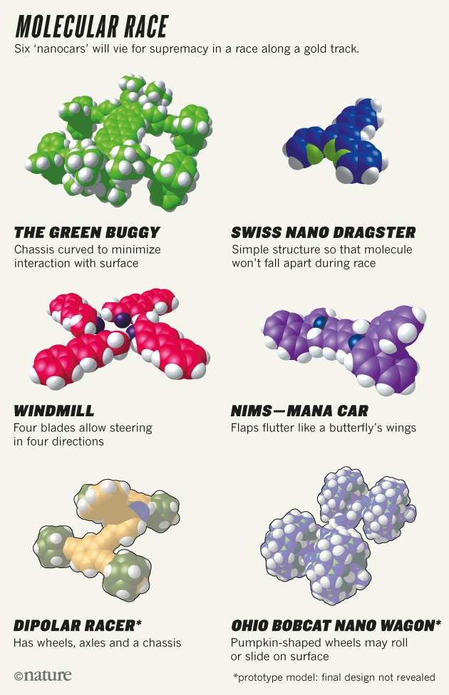
An April 19, 2017 article by Davide Castelvecchi for Nature (magazine) provided more detail about the race (Note: Links have been removed),
The term nanocar is actually a misnomer, because the molecules involved in this race have no motors. (Future races may incorporate them, Joachim says.) And it is not clear whether the molecules will even roll along like wagons: a few designs might, but many lack axles and wheels. Drivers will use electrons from the tip of a scanning tunnelling microscope (STM) to help jolt their molecules along, typically by just 0.3 nano-metres each time — making 100 nanometres “a pretty long distance”, notes physicist Leonhard Grill of the University of Graz, Austria, who co-leads a US–Austrian team in the race.
Contestants are not allowed to directly push on their molecules with the STM tip. Some teams have designed their molecules so that the incoming electrons raise their energy states, causing vibrations or changes to molecular structures that jolt the racers along. Others expect electrostatic repulsion from the electrons to be the main driving force. Waka Nakanishi, an organic chemist at the National Institute for Materials Science in Tsukuba, Japan, has designed a nanocar with two sets of ‘flaps’ that are intended to flutter like butterfly wings when the molecule is energized by the STM tip (see ‘Molecular race’). Part of the reason for entering the race, she says, was to gain access to the Toulouse lab’s state-of-the-art STM to better understand the molecule’s behaviour.
Eric Masson, a chemist at Ohio University in Athens, hopes to find out whether the ‘wheels’ (pumpkin-shaped groups of atoms) of his team’s car will roll on the surface or simply slide. “We want to better understand the nature of the interaction between the molecule and the surface,” says Masson..
Adapted from www.nanocar-race.cnrs.fr
Simply watching the race progress is half the battle. After each attempted jolt, teams will take three minutes to scan their race track with the STM, and after each hour they will produce a short animation that will immediately be posted online. That way, says Joachim, everyone will be able to see the race streamed almost live.
Nanoscale races
…
The Toulouse laboratory has an unusual STM with four scanning tips — most have only one — that will allow four teams to race at the same time, each on a different section of the gold surface. Six teams will compete this week to qualify for one of the four spots; the final race will begin on 28 April at 11 a.m. local time. The competitors will face many obstacles during the contest. Individual molecules in the race will often be lost or get stuck, and the trickiest part may be to negotiate the two turns in the track, Joachim says. He thinks the racers may require multiple restarts to cover the distance.
For anyone who wants more information, go to the Nanocar Race website. There is also a highlights video,
Published on Apr 29, 2017
The best moments of the first-ever international race of molecule- cars.
One of the issues with new materials is being able to produce them in a commercially viable fashion and it seems that researchers in Australia may have helped to do that with graphene. From a Feb. 15, 2017 news item on phys.org,
A breakthrough by CSIRO-led [Australia’s Commonwealth Scientific and Industrial Research Organisation] scientists has made the world’s strongest material more commercially viable, thanks to the humble soybean.
Graphene is a carbon material that is one atom thick.
Its thin composition and high conductivity means it is used in applications ranging from miniaturised electronics to biomedical devices.
These properties also enable thinner wire connections; providing extensive benefits for computers, solar panels, batteries, sensors and other devices.
Until now, the high cost of graphene production has been the major roadblock in its commercialisation.
Previously, graphene was grown in a highly-controlled environment with explosive compressed gases, requiring long hours of operation at high temperatures and extensive vacuum processing.
CSIRO scientists have developed a novel “GraphAir” technology which eliminates the need for such a highly-controlled environment.
The technology grows graphene film in ambient air with a natural precursor, making its production faster and simpler.
“This ambient-air process for graphene fabrication is fast, simple, safe, potentially scalable, and integration-friendly,” CSIRO scientist Dr Zhao Jun Han, co-author of the paper published today in Nature Communications said.
“Our unique technology is expected to reduce the cost of graphene production and improve the uptake in new applications.”
GraphAir transforms soybean oil – a renewable, natural material – into graphene films in a single step.
“Our GraphAir technology results in good and transformable graphene properties, comparable to graphene made by conventional methods,” CSIRO scientist and co-author of the study Dr Dong Han Seo said.
With heat, soybean oil breaks down into a range of carbon building units that are essential for the synthesis of graphene.
The team also transformed other types of renewable and even waste oil, such as those leftover from barbecues or cooking, into graphene films.
“We can now recycle waste oils that would have otherwise been discarded and transform them into something useful,” Dr Seo said.
The potential applications of graphene include water filtration and purification, renewable energy, sensors, personalised healthcare and medicine, to name a few.
Graphene has excellent electronic, mechanical, thermal and optical properties as well.
Its uses range from improving battery performance in energy devices, to cheaper solar panels.
CSIRO are looking to partner with industry to find new uses for graphene.
Researchers from The University of Sydney, University of Technology Sydney and The Queensland University of Technology also contributed to this work.
Physicists at Kansas State University use controlled detonation to make graphene according to a Jan. 25, 2017 news item on Nanowerk (Note: A link has been removed),
Forget chemicals, catalysts and expensive machinery — a Kansas State University team of physicists has discovered a way to mass-produce graphene with three ingredients: hydrocarbon gas, oxygen and a spark plug.
Their method is simple: Fill a chamber with acetylene or ethylene gas and oxygen. Use a vehicle spark plug to create a contained detonation. Collect the graphene that forms afterward.
Chris Sorensen, Cortelyou-Rust university distinguished professor of physics, is the lead inventor of the recently issued patent, “Process for high-yield production of graphene via detonation of carbon-containing material”. Other Kansas State University researchers involved include Arjun Nepal, postdoctoral researcher and instructor of physics, and Gajendra Prasad Singh, former visiting scientist.
“We have discovered a viable process to make graphene,” Sorensen said. “Our process has many positive properties, from the economic feasibility, the possibility for large-scale production and the lack of nasty chemicals. What might be the best property of all is that the energy required to make a gram of graphene through our process is much less than other processes because all it takes is a single spark.”
Graphene is a single atom-thick sheet of hexagonally coordinated carbon atoms, which makes it the world’s thinnest material. Since graphene was isolated in 2004, scientists have found it has valuable physical and electronic properties with many possible applications, such as more efficient rechargeable batteries or better electronics.
For Sorensen’s research team, the serendipitous path to creating graphene started when they were developing and patenting carbon soot aerosol gels. They created the gels by filling a 17-liter aluminum chamber with acetylene gas and oxygen. Using a spark plug, they created a detonation in the chamber. The soot from the detonation formed aerosol gels that looked like “black angel food cake,” Sorensen said.
But after further analysis, the researchers found that the aerosol gel was more than lookalike dark angel food cake — it was graphene.
“We made graphene by serendipity,” Sorensen said. “We didn’t plan on making graphene. We planned on making the aerosol gel and we got lucky.”
But unlike other methods of creating graphene, Sorensen’s method is simple, efficient, low-cost and scalable for industry.
Other methods of creating graphene involve “cooking” the mineral graphite with chemicals — such as sulfuric acid, sodium nitrate, potassium permanganate or hydrazine — for a long time at precisely prescribed temperatures. Additional methods involve heating hydrocarbons to 1,000 degrees Celsius in the presence of catalysts.
Such methods are energy intensive — and even dangerous — and have low yield, while Sorensen and his team’s method makes larger quantities with minimal energy and no dangerous chemicals.
“The real charm of our experiment is that we can produce graphene in the quantity of grams rather than milligrams,” Nepal said.
Now the research team — including Justin Wright, doctoral student in physics, Camp Hill, Pennsylvania — is working to improve the quality of the graphene and scale the laboratory process to an industrial level. They are upgrading some of the equipment to make it easier to get graphene from the chamber seconds — rather than minutes — after the detonation. Accessing the graphene more quickly could improve the quality of the material, Sorensen said.
The patent was issued to the Kansas State University Research Foundation, a nonprofit corporation responsible for managing technology transfer activities at the university.
I wish they’d filmed one of their graphene explosions even if it meant that all we’d get is the sight of a canister and the sound of a boom. Still, they did show a brief spark from the spark plug.
… the path to greater benefits – whether economic, social, or environmental – from nanomanufactured goods and services is not yet clear. A recent review article in ACS Nano (“Nanomanufacturing: A Perspective”) by J. Alexander Liddle and Gregg M. Gallatin, takes silicon integrated circuit manufacturing as a baseline in order to consider the factors involved in matching processes with products, examining the characteristics and potential of top-down and bottom-up processes, and their combination.
The authors also discuss how a careful assessment of the way in which function can be made to follow form can enable high-volume manufacturing of nanoscale structures with the desired useful, and exciting, properties.
Although often used interchangeably, it makes sense to distinguish between nanofabrication and nanomanufacturing using the criterion of economic viability, suggested by the connotations of industrial scale and profitability associated with the word ‘manufacturing’.
Here’s a link to and a citation for the paper Berger is reviewing,
Nanomanufacturing: A Perspective by J. Alexander Liddle and Gregg M. Gallatin. ACS Nano, 2016, 10 (3), pp 2995–3014 DOI: 10.1021/acsnano.5b03299 Publication Date (Web): February 10, 2016
Copyright This article not subject to U.S. Copyright. Published 2016 by the American Chemical Society
This paper is behind a paywall.
Luckily for those who’d like a little more information before purchase, Berger’s review provides some insight into the study additional to what you’ll find in the abstract,
Nanomanufacturing, as the authors define it in their article, therefore, has the salient characteristic of being a source of money, while nanofabrication is often a sink.
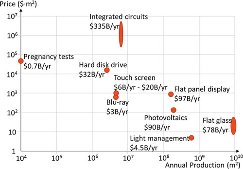
To supply some background and indicate the scale of the nanomanufacturing challenge, the figure below shows the selling price ($·m-2) versus the annual production (m2) for a variety of nanoenabled or potentially nanoenabled products. The overall global market sizes are also indicated. It is interesting to note that the selling price spans 5 orders of magnitude, the production six, and the market size three. Although there is no strong correlation between the variables,
market price and size nanoenabled product
Log-log plot of the approximate product selling price ($·m-2) versus global annual production (m2) for a variety of nanoenabled, or potentially nanoenabled products. Approximate market sizes (2014) are shown next to each point. (Reprinted with permission by American Chemical Society)
Log-log plot of the approximate product selling price ($·m-2) versus global annual production (m2) for a variety of nanoenabled, or potentially nanoenabled products. Approximate market sizes (2014) are shown next to each point. (Reprinted with permission by American Chemical Society)
I encourage anyone interested in nanomanufacturing to read Berger’s article in its entirety as there is more detail and there are more figures to illustrate the points being made. He ends his review with this,
“Perhaps the most exciting prospect is that of creating dynamical nanoscale systems that are capable of exhibiting much richer structures and functionality. Whether this is achieved by learning how to control and engineer biological systems directly, or by building systems based on the same principles, remains to be seen, but will undoubtedly be disruptive and quite probably revolutionary.”
I find the reference to biological systems quite interesting especially in light of the recent launch of DARPA’s (US Defense Advanced Research Projects Agency) Engineered Living Materials (ELM) program (see my Aug. 9, 2016 posting).
It’s a bit puzzling initially as both the SHYMAN (Sustainable Hydrothermal Manufacturing of Nanomaterials) project and Promethean Particles are claiming to be the world’s biggest nanomaterials production facility. In a battle of press release titles (one from CORDIS and one from the University of Nottingham) it becomes clear after reading both that the SHYMAN project is the name for a European Commission 7th Framework Programme funded project and Promethean Particles, located at the University of Nottingham (UK), is a spinoff from that project. So, both claims are true, although confusing at first glance.
An Aug. 1, 2016 news item on Nanowerk breaks the news about the ‘SHYMAN project’s’ production facility (Note: A link has been removed),
The European SHYMAN project aims to establish continuous hydrothermal synthesis as the most flexible and sustainable process to create nanomaterials at industrial scale. After demonstrating this potential in the lab, the project has now announced the opening of its first facility in Nottingham.
‘This new facility opens up a significant amount of new opportunities for us,’ says Professor Ed Lester, Technical Coordinator of Promethean Particles. This spin-out of the University of Nottingham is in charge of operating the new plant, which is expected to produce over 1 000 tonnes of nanomaterials every year. The production cost is lower than that of other facilities and the chosen production method – continuous hydrothermal synthesis – is expected to impact even markets for which sale prices had so far been an obstacle.
‘We have already had a lot of interest from companies in a diverse range of sectors. From healthcare, where nano-particles can be used in coatings on medical devices, to enhanced fabrics, where nano-materials can add strength and flexibility to textiles, and in printed electronics, as we are able to print materials such as copper,’ Prof. Lester continues. Solvay, Fiat, PPG and Repsol are among the major companies already set to benefit from the plant’s products.
To reach these impressive levels of production, the plant notably relies on high pressure triplex plunger pumps manufactured by Cat Pumps. These pumps have helped the 18-strong consortium to overcome engineering issues related to the mixing of the heated fluid and the aqueous metal salt flow, by creating the continuous pressure and fluid flow necessary to achieve continuous production.
Another enabling technology is the Nozzle Reactor, a customised design that uses buoyancy-induced eddies to produce an ‘ideal’ mixing scenario in a pipe-in-pip concentric configuration in which the internal pipe has an open-ended nozzle. This technology allows Promethean Particles to dramatically improve reproducibility and reliability whilst controlling particles properties such as size, composition and shape.
Betting on hydrothermal synthesis
Started in 2012, SHYMAN built upon the observation that hydrothermal synthesis had numerous advantages compared to alternatives: it doesn’t resort to noxious chemicals, uses relatively simple chemistry relying on cheap precursors, allows straightforward downstream processing, can avoid agglomeration and allows for narrow and well-controlled size and shape distribution.
The optimisation of hydrothermal synthesis has been a key objective of the University of Nottingham for the past 14 years, and SHYMAN is the pinnacle: the project began with the development of bench scale reactors, followed by a 30-times-larger pilot scale reactor. The reactor at the heart of the new production plant is 80 times larger than the latter and features four Cat Pumps Model 3801 high pressure triplex plunger pumps.
‘These are very exciting times for Promethean Particles,’ said Dr Susan Huxtable, Director of Intellectual Property and Commercialisation at the University of Nottingham. ‘The new facility opens up a myriad of opportunities for them to sell their services into new markets right across the world. It is a great example of how many of the technologies developed by academics here at the University of Nottingham have the potential to benefit both industry and society.’
The plant [Promethean Particles] was developed as part of a pan-European nano-materials research programme, known as SHYMAN (Sustainable Hydrothermal Manufacturing of Nanomaterials). The project, which had a total value of €9.7 million Euros, included partner universities and businesses from 12 European countries.
…
The outcome of the project was the creation of the largest multi-material nano-particle plant in the world, based in Nottingham. The plant is now operated by Promethean, and it is able to operate at supercritical conditions, producing up to 200 kg of nano-particles per hour.
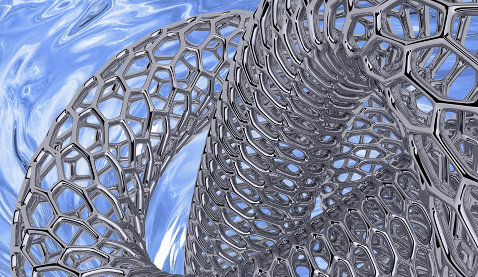
Carbon nanotubes can be wiggly, entangled things (more about McMaster in a bit) as Dr. Andrew Maynard notes in this video (part of his Risk Bites video series) describing carbon nanotubes, their ‘infinite’ variety, and risks,
Researchers at Canada’s McMaster University have found a way to untangle carbon nanotubes according to an Aug. 16, 2016 news item on Nanowerk (Note: A link has been removed),
Imagine an electronic newspaper that you could roll up and spill your coffee on, even as it updated itself before your eyes.
It’s an example of the technological revolution that has been waiting to happen, except for one major problem that, until now, scientists have not been able to resolve.
Researchers at McMaster University have cleared that obstacle by developing a new way to purify carbon nanotubes – the smaller, nimbler semiconductors that are expected to replace silicon within computer chips and a wide array of electronics (Chemistry – A European Journal, “Influence of Polymer Electronics on Selective Dispersion of Single-Walled Carbon Nanotubes”).
“Once we have a reliable source of pure nanotubes that are not very expensive, a lot can happen very quickly,” says Alex Adronov, a professor of Chemistry at McMaster whose research team has developed a new and potentially cost-efficient way to purify carbon nanotubes.
The researchers have provided a gorgeous image,
Artistic rendition of a metallic carbon nanotube being pulled into solution, in analogy to the work described by the Adronov group. Image: Alex Adronov McMaster University
An Aug. 15, 2016 McMaster University news release, which originated the news item, provides a beginner’s introduction to carbon nanotubes and describes the purification process that will make production of carbon nanotubes easier,
Carbon nanotubes – hair-like structures that are one billionth of a metre in diameter but thousands of times longer – are tiny, flexible conductive nano-scale materials, expected to revolutionize computers and electronics by replacing much larger silicon-based chips.
A major problem standing in the way of the new technology, however, has been untangling metallic and semiconducting carbon nanotubes, since both are created simultaneously in the process of producing the microscopic structures, which typically involves heating carbon-based gases to a point where mixed clusters of nanotubes form spontaneously as black soot.
Only pure semiconducting or metallic carbon nanotubes are effective in device applications, but efficiently isolating them has proven to be a challenging problem to overcome. Even when the nanotube soot is ground down, semiconducting and metallic nanotubes are knotted together within each grain of powder. Both components are valuable, but only when separated.
Researchers around the world have spent years trying to find effective and efficient ways to isolate carbon nanotubes and unleash their value.
While previous researchers had created polymers that could allow semiconducting carbon nanotubes to be dissolved and washed away, leaving metallic nanotubes behind, there was no such process for doing the opposite: dispersing the metallic nanotubes and leaving behind the semiconducting structures.
Now, Adronov’s research group has managed to reverse the electronic characteristics of a polymer known to disperse semiconducting nanotubes – while leaving the rest of the polymer’s structure intact. By so doing, they have reversed the process, leaving the semiconducting nanotubes behind while making it possible to disperse the metallic nanotubes.
The researchers worked closely with experts and equipment from McMaster’s Faculty of Engineering and the Canada Centre for Electron Microscopy, located on the university’s campus.
“There aren’t many places in the world where you can do this type of interdisciplinary work,” Adronov says.
The next step, he explains, is for his team or other researchers to exploit the discovery by finding a way to develop even more efficient polymers and scale up the process for commercial production.