Monthly Archives: June 2015

Silk inks containing enzymes, antibiotics, antibodies, nanoparticles, and growth factors

There’s an almost euphoric tone to a June 16, 2015 Tufts University news release (also on EurekAlert) about research which has resulted in the ability to print silk-based inks,

Silk inks containing enzymes, antibiotics, antibodies, nanoparticles and growth factors could turn inkjet printing into a new, more effective tool for therapeutics, regenerative medicine and biosensing, according to new research led by Tufts University  biomedical engineers and published June 16 [2015] in the journal Advanced Materials online in advance of print.

Until now, heat used in the inkjet printing process made using silk a challenge (as it does for cellulose nanomaterials used in 3D printers, noted in my June 17, 2015 posting), from the Tufts news release,

Inkjet printing is one of the most immediate and accessible forms of printing technology currently available, according to the researchers, and ink-jet printing of biomolecules has been previously proposed by scientists. However, the heat-sensitive nature of these unstable compounds means printed materials rapidly lose functionality, limiting their use.

Enter purified silk protein, or fibroin, which offers intrinsic strength and protective properties that make it well-suited for a range of biomedical and optoelectronic applications. This natural polymer is an ideal “cocoon” that can stabilize compounds such as enzymes, antibodies and growth factors while lending itself to many different mechanically robust formats, said Fiorenzo Omenetto, Ph.D., senior author on the paper and associate dean for research and Frank C. Doble Professor of Engineering at Tufts School of Engineering.

“We thought that if we were able to develop an inkjet-printable silk solution, we would have a universal building block to generate multiple functional printed formats that could lead to a wide variety of applications in which inks remain active over time,” he said.

By using this simple approach and starting with the same base material, the research team created and tested a “custom library” of inkjet-printable, functional silk inks doped with a variety of components:

  • Bacterial-sensing polydiacetylenes (PDAs) printed on surgical gloves; the word “contaminated” printed on the glove changed from blue to red after exposure to E. coli
  • Proteins that stimulate bone growth (BMP-2) printed on a plastic dish to test topographical control of directed tissue growth
  • Sodium ampicillin printed on a bacterial culture to test the effectiveness of a topographical distribution of the antibiotic
  • Gold nanoparticles printed on paper, for possible application in photonics and biology (e.g., color engineering, surface plasmon resonance based sensing and bio-imaging)
  • Enzymes printed on paper to test the ability of the ink to entrain small functional biomolecules

The researchers, who included collaborators from the University of Illinois at Urbana-Champaign, foresee wide potential for future investigation and application of this technology.

For example, Omenetto envisions more work on the bio-sensing gloves, which he says could selectively react to different pathological agents. The ability to print antibiotics in topographical patterns could address the need for “smart” bandages, where therapeutics are incorporated and delivered to match a complex injury.

The published research was restricted to one ink cartridge, but the scientists believe it could extend to multi-cartridge printing combining complex functions.

Omenetto and Kaplan are pioneers in the use of silk as an alternative to plastics. Omenetto’s 2011 TED Talk called silk a “new old material” that could have a profound impact in many technical fields.

Here’s a link to and citation for the paper,

Inkjet Printing of Regenerated Silk Fibroin: From Printable Forms to Printable Functions by Hu Tao, Benedetto marelli, Miaomiao Yang, Bo An, Serdar Onses, John A. Rogers, David L. Kaplan, & Fiorenzo G. Omenetto. Advanced Materials DOI: 10.1002/adma.201501425 First published: 16 June 2015

This article is behind a paywall.

Not origami but kirigami-inspired foldable batteries

Origami is not noted for its stretchy qualities, a shortcoming according to a June 16, 2015 news item on Azonano,

Origami, the centuries-old Japanese paper-folding art, has inspired recent designs for flexible energy-storage technology. But energy-storage device architecture based on origami patterns has so far been able to yield batteries that can change only from simple folded to unfolded positions. They can flex, but not actually stretch.

Now an Arizona State University [ASU] research team has overcome the limitation by using a variation of origami, called kirigami, as a design template for batteries that can be stretched to more than 150 percent of their original size and still maintain full functionality.

A June 15, 2015 ASU news release, which originated the news item, provides a few more details about the kirigami-influenced batteries (Note: A link has been removed),

A paper published on June 11 [2015] in the research journal Scientific Reports describes how the team developed kirigami-based lithium-ion batteries using a combination of folds and cuts to create patterns that enable a significant increase in stretchability.

The kirigami-based prototype battery was sewn into an elastic wristband that was attached to a smart watch. The battery fully powered the watch and its functions – including playing video – as the band was being stretched.

“This type of battery could potentially be used to replace the bulky and rigid batteries that are limiting the development of compact wearable electronic devices,” Jiang said.

Such stretchable batteries could even be integrated into fabrics – including those used for clothing, he said.

The researchers have provided a video demonstrating the kirigami-inspired battery in action,

Here’s a link to and a citation for the paper,

Kirigami-based stretchable lithium-ion batteries by Zeming Song, Xu Wang, Cheng Lv, Yonghao An, Mengbing Liang, Teng Ma, David He, Ying-Jie Zheng, Shi-Qing Huang, Hongyu Yu & Hanqing Jiang. Scientific Reports 5, Article number: 10988 doi:10.1038/srep10988 Published 11 June 2015

This is an open access paper.

According to the ASU news release, the team published a previous paper on origami-inspired batteries and some of the problems associated with them (Note: Links have been removed),

An earlier paper in the research journal Nature Communications by Jiang and some of his research team members and other colleagues provides an in-depth look at progress and obstacles in the development of origami-based lithium-ion batteries.

The paper explains technical challenges in flexible-battery development that Jiang says his team’s kirigami-based devices are helping to solve.

Read more about the team’s recent progress and the potential applications of stretchable batteries in Popular Mechanics, the Christian Science Monitor, Yahoo News and the Daily Mail.

Here’s a link to and a citation for the team’s earlier paper,

Origami lithium-ion batteries by Zeming Song, Teng Ma,    Rui Tang, Qian Cheng, Xu Wang, Deepakshyam Krishnaraju, Rahul Panat, Candace K. Chan, Hongyu Yu, & Hanqing Jiang. Nature Communications 5, Article number: 3140 doi:10.1038/ncomms4140 Published 28 January 2014

This paper is behind a paywall but there is a free preview available via ReadCube Access.

On a related note, Dexter Johnson has written up Binghamton University research into paper-based origami batteries powered by the respiration of bacteria in a June 16, 2015 posting on his Nanoclast blog.

Japanese researchers note the emergence of the ‘Devil’s staircase’

I wanted to know why it’s called the ‘Devil’s staircase’ and this is what I found. According to Wikipedia there are several of them,

I gather the scientists are referring to the Cantor function (mathematics), Note: Links have been removed,

In mathematics, the Cantor function is an example of a function that is continuous, but not absolutely continuous. It is also referred to as the Cantor ternary function, the Lebesgue function, Lebesgue’s singular function, the Cantor-Vitali function, the Devil’s staircase,[1] the Cantor staircase function,[2] and the Cantor-Lebesgue function.[3]

Here’s a diagram illustrating the Cantor function (from the Wikipedia entry),

CC BY-SA 3.0 File:CantorEscalier.svg Uploaded by Theon Created: January 24, 2009

CC BY-SA 3.0
File:CantorEscalier.svg
Uploaded by Theon
Created: January 24, 2009

As for this latest ‘Devil’s staircase’, a June 17, 2015 news item on Nanowerk announces the research (Note: A link has been removed),

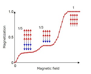
Researchers at the University of Tokyo have revealed a novel magnetic structure named the “Devil’s staircase” in cobalt oxides using soft X-rays (“Observation of a Devil’s Staircase in the Novel Spin-Valve System SrCo6O11“). This is an important result since the researchers succeeded in determining the detailed magnetic structure of a very small single crystal invisible to the human eye.

A June 17, 2015 University of Tokyo press release, which originated the news item on Nanowerk, describes why this research is now possible and the impact it could have,

Recent remarkable progress in resonant soft x-ray diffraction performed in synchrotron facilities has made it possible to determine spin ordering (magnetic structure) in small-volume samples including thin films and nanostructures, and thus is expected to lead not only to advances in materials science but also application to spintronics, a technology which is expected to form the basis of future electronic devices. Cobalt oxide is known as one material that is suitable for spintronics applications, but its magnetic structure was not fully understood.

The research group of Associate Professor Hiroki Wada at the University of Tokyo Institute for Solid State Physics, together with the researchers at Kyoto University and in Germany, performed a resonant soft X-ray diffraction study of cobalt (Co) oxides in the synchrotron facility BESSY II in Germany. They observed all the spin orderings which are theoretically possible and determined how these orderings change with the application of magnetic fields. The plateau-like behavior of magnetic structure as a function of magnetic field is called the “Devil’s staircase,” and is the first such discovery in spin systems in 3D transition metal oxides including cobalt, iron, manganese.

By further resonant soft X-ray diffraction studies, one can expect to find similar “Devil’s staircase” behavior in other materials. By increasing the spatial resolution of microscopic observation of the “Devil’s staircase” may lead to the development of novel types of spintronics materials.

Here’s an example of the ‘cobalt’ Devil’s staircase,

The magnetic structure that gives rise to the Devil's Staircase Magnetization (vertical axis) of cobalt oxide shows plateau like behaviors as a function of the externally-applied magnetic field (horizontal axis). The researchers succeeded in determining the magnetic structures which create such plateaus. Red and blue arrows indicate spin direction. © 2015 Hiroki Wadati.

The magnetic structure that gives rise to the Devil’s Staircase
Magnetization (vertical axis) of cobalt oxide shows plateau like behaviors as a function of the externally-applied magnetic field (horizontal axis). The researchers succeeded in determining the magnetic structures which create such plateaus. Red and blue arrows indicate spin direction.
© 2015 Hiroki Wadati.

Here’s a link to and a citation for the paper,

Observation of a Devil’s Staircase in the Novel Spin-Valve System SrCo6O11 by T. Matsuda, S. Partzsch, T. Tsuyama, E. Schierle, E. Weschke, J. Geck, T. Saito, S. Ishiwata, Y. Tokura, and H. Wadati. Phys. Rev. Lett. 114, 236403 – Published 11 June 2015 (paper: Vol. 114, Iss. 23 — 12 June 2015)  DOI: 10.1103/PhysRevLett.114.236403

This paper is behind a paywall.

Science pledge for Canadians launched on June 16, 2015 and a flashback to political parties and Canadian science policy (a lack of it)

H/t to Speaking Up For Canadian Science.

As noted in a previous post, I’m not super impressed with the ‘War on Science’ branding favoured by a distinct portion of the Canadian science community as I find it reductionist. After all, Canada’s current Conservative government is perfectly happy with certain kinds of science, just not climate science, most of the biological sciences, environmental sciences, … (I imagine you’ve gotten the drift). That said, I am sympathetic (admittedly self-serving) to the concerns over the government’s antipathy towards science communication of all kinds.

The latest news about the movement to change the attitude to many Canadian science efforts comes from a June 16, 2015 article by Fram Dinshaw for the National Observer,

Federal MPs from three opposition parties signed a pledge in support of science-driven policies after recent protests by federal scientists against the Harper government’s cuts to departments and its muzzling of research.

Signing on at the June 16 [2015] press conference by Evidence for Democracy were NDP’s Kennedy Stewart, the official opposition’s science and technology critic, Liberal MP and former astronaut Marc Garneau, and Green Party leader Elizabeth May.

Stewart has already tabled three bills before parliament to restore Ottawa’s scientific capacity, including restoration of the long form census, an ethical code to end muzzling of scientists, and the creation of a parliamentary science officer with the powers of an auditor-general.

Evidence for Democracy is pushing back in the run-up to October’s federal election by promoting the implementation of a new government-wide communications policy to ensure that government scientists can speak publicly about their research and creating a new federal science office to advise decision-makers, according to a media release dated June 16.

“Scientists are now supporting this issue publicly,” Dr. Katie Gibbs, Executive Director of Evidence for Democracy, said. “To my knowledge this is the first time Canadian scientists have mobilized to promote science as a federal election issue. The Pledge invites Parliamentarians and the broader community show their support for public-interest science and evidence-based decision-making.”

“The trends we’ve seen in recent years are deeply troubling to many in the scientific community,” Dr. Scott Findlay, Associate Professor of Biology at the University of Ottawa and Evidence for Democracy Board member, said. Trends include, “funding cuts to science, government scientists not being able to speak about their work, and decisions that appear to play fast and loose with scientific evidence.”

You can find Evidence for Democracy’s Science Pledge here.

Science policy flashback

One of my first science policy posts was a January 15, 2010 piece where I tried to find science policies for Canada’s four main political parties (Liberals, New Democrats [NDP], Conservatives, and Greens). The only party that mentioned science policy was the Conservative Party.

I followed up that first post with one dated January 22, 2010 where I tracked down then official ‘science’ critics for each party (Liberals, Marc Garneau; Greens, Frances Coates; and New Democrats, Jim Malloway) and the Ministry of State for Science and Technology (Conservative Member of Parliament, Gary Goodyear) and tried to find something about science on their websites and in their writings. Garneau was the only Member of Parliament to mention science. In fact, he’d written a science policy on his own.

The last election year (2011) produced a few posts on political parties and science policies. I’m particularly fond of my April 18, 2011 post,

It’s only in my dreams or, perhaps, my nightmares that science policy is considered an important issue in a Canadian federal election. Being an election issue can be a two-edged sword, you get more attention but that can work for you and/or against you. On balance, I think it’s better to be considered an election issue than to be ignored and it seems to me that there’s a lot more effort (not from the political parties) this election to put science policy in the limelight.

I posted two followups: April 26, 2011 (it features a visualization of the issues in the 2011 election; science did not rate a placement in the graphic) and April 29, 2011.

Things have changed since those first science policy posts. Some of the changes have been influenced by the international zeitgeist and some by individuals such as Pascal Lapointe and his team members at Agence Science- Presse in Québec, by politicians newly concerned about science issues, and new Canadian science organizations with  political outlooks such as Evidence for Democracy and Speak Up For Canadian Science, and, of course, individual scientists themselves.

South American countries and others visit Iran’s Nanotechnology Initiative Council

The Iran Nanotechnology Initiative Council (INIC) news release states eight South American countries visited. By my count there were six South American countries (Argentina, Brazil, Ecuador, Bolivia, Venezuela, and Uruguay,), one North American country (Mexico), and one Caribbean country (Cuba). All eight can be described as Latin American countries.

An easy to understand error (I once forgot Mexico is part of North America and, for heaven sakes, I live in Canada and really should know better) as the designations can be confusing. That cleared up, here’s what the June 15, 2015 INIC news release had to say about the visit,

The ambassadors and charge d’affaires of 8 South American countries of Argentina, Brazil, Ecuador, Bolivia, Cuba, Venezuela, Uruguay and Mexico paid a visit to Iran Nanotechnology Initiative Council (INIC) to become familiar with its activities.

Among the objectives of the visit, which was requested by the abovementioned countries, mention can be made of introduction with INIC and its activities, presentation of nanotechnology achievements and products in the country by the INIC, creation and modification of international cooperation and creation of appropriate environment for exporting nanotechnology-based products to these countries.

In this visit, the programs, achievements and objectives of nanotechnology development in Iran were explained by the authorities of INIC. In addition and due to the needs of the countries whose representatives were present in the visit, a number of experts from the Iranian knowledge-based companies presented their nanotechnology products in the fields of packaging of agricultural products with long durability and water purification.

As usual with something from INIC, I long for more detail, e.g., when did the visit take place?

H/t to Nanotechnology Now June 15, 2015 news item.

Courtesy of graphene: world’s thinnest light bulb

Columbia University’s (US) School of Engineering and Applied Science is trumpeting an achievement with graphene, i.e., the world’s thinnest light bulb. From a June 15, 2015 Columbia Engineering news release (also on EurekAlert),

Led by Young Duck Kim, a postdoctoral research scientist in James Hone’s group at Columbia Engineering, a team of scientists from Columbia, Seoul National University (SNU), and Korea Research Institute of Standards and Science (KRISS) reported today that they have demonstrated — for the first time — an on-chip visible light source using graphene, an atomically thin and perfectly crystalline form of carbon, as a filament. They attached small strips of graphene to metal electrodes, suspended the strips above the substrate, and passed a current through the filaments to cause them to heat up.

“We’ve created what is essentially the world’s thinnest light bulb,” says Hone, Wang Fon-Jen Professor of Mechanical Engineering at Columbia Engineering and coauthor of the study. “This new type of ‘broadband’ light emitter can be integrated into chips and will pave the way towards the realization of atomically thin, flexible, and transparent displays, and graphene-based on-chip optical communications.”

The news release goes on to describe some of the issues associated with generating light on a chip and how the researchers approached the problems (quick answer: they used graphene as the filament),

Creating light in small structures on the surface of a chip is crucial for developing fully integrated “photonic” circuits that do with light what is now done with electric currents in semiconductor integrated circuits. Researchers have developed many approaches to do this, but have not yet been able to put the oldest and simplest artificial light source—the incandescent light bulb—onto a chip. This is primarily because light bulb filaments must be extremely hot—thousands of degrees Celsius—in order to glow in the visible range and micro-scale metal wires cannot withstand such temperatures. In addition, heat transfer from the hot filament to its surroundings is extremely efficient at the microscale, making such structures impractical and leading to damage of the surrounding chip.

By measuring the spectrum of the light emitted from the graphene, the team was able to show that the graphene was reaching temperatures of above 2500 degrees Celsius, hot enough to glow brightly. “The visible light from atomically thin graphene is so intense that it is visible even to the naked eye, without any additional magnification,” explains Kim, first and co-lead author on the paper.

Interestingly, the spectrum of the emitted light showed peaks at specific wavelengths, which the team discovered was due to interference between the light emitted directly from the graphene and light reflecting off the silicon substrate and passing back through the graphene. Kim notes, “This is only possible because graphene is transparent, unlike any conventional filament, and allows us to tune the emission spectrum by changing the distance to the substrate.”

The ability of graphene to achieve such high temperatures without melting the substrate or the metal electrodes is due to another interesting property: as it heats up, graphene becomes a much poorer conductor of heat. This means that the high temperatures stay confined to a small “hot spot” in the center.

“At the highest temperatures, the electron temperature is much higher than that of acoustic vibrational modes of the graphene lattice, so that less energy is needed to attain temperatures needed for visible light emission,” Myung-Ho Bae, a senior researcher at KRISS and co-lead author, observes. “These unique thermal properties allow us to heat the suspended graphene up to half of the temperature of the sun, and improve efficiency 1000 times, as compared to graphene on a solid substrate.”

The team also demonstrated the scalability of their technique by realizing large-scale of arrays of chemical-vapor-deposited (CVD) graphene light emitters.

Yun Daniel Park, professor in the Department of Physics and Astronomy at Seoul National University and co-lead author, notes that they are working with the same material that Thomas Edison used when he invented the incandescent light bulb: “Edison originally used carbon as a filament for his light bulb and here we are going back to the same element, but using it in its pure form—graphene—and at its ultimate size limit—one atom thick.”

The group is currently working to further characterize the performance of these devices—for example, how fast they can be turned on and off to create “bits” for optical communications—and to develop techniques for integrating them into flexible substrates.

Hone adds, “We are just starting to dream about other uses for these structures—for example, as micro-hotplates that can be heated to thousands of degrees in a fraction of a second to study high-temperature chemical reactions or catalysis.”

Here’s a link to and a citation for the paper,

Bright visible light emission from graphene by Young Duck Kim, Hakseong Kim, Yujin Cho, Ji Hoon Ryoo, Cheol-Hwan Park, Pilkwang Kim, Yong Seung Kim, Sunwoo Lee, Yilei Li, Seung-Nam Park, Yong Shim Yoo, Duhee Yoon, Vincent E. Dorgan, Eric Pop, Tony F. Heinz, James Hone, Seung-Hyun Chun, Hyeonsik Cheong, Sang Wook Lee,    Myung-Ho Bae, & Yun Daniel Park. Nature Nanotechnology (2015) doi:10.1038/nnano.2015.118 Published online 15 June 2015

This paper is behind a paywall.

Two final notes: there was an announcement earlier this year (mentioned in my March 30, 2015 post) that a graphene light bulb would be in stores this year. Dexter Johnson notes in his June 15, 2015 post (Nanoclast blog on the IEEE [International Institute of Electrical and Electronics Engineers] website) that the earlier light bulb has a graphene coating. You may want to check out Dexter’s posting about the latest light bulb achievement as he also includes an embedded video illustrating how Columbia Engineering’s graphene filament works.

Platinum catalysts and their shortcomings

The problem boils down to the fact that platinum isn’t cheap and so US Dept. of Energy research laboratories are looking for alternatives to or ways of making more efficient use of platinum according to a June 16, 2015 news item on Nanowerk,

Visions of dazzling engagement rings may pop to mind when platinum is mentioned, but a significant share of the nearly half a million pounds of the rare metalExternal link [sic] mined each year ends up in vehicle emission systems and chemical manufacturing plants. The silvery white metal speeds up or enhances reactions, a role scientists call serving as a catalyst, and platinum is fast and efficient performing this function.

Because of its outstanding performance as a catalyst, platinum plays a major role in fuel cells. Inside a fuel cell, tiny platinum particles break apart hydrogen fuel to create electricity. Leftover protons are combined with oxygen ions to create pure water.

Fuel cells could let scientists turn wind into fuel. Right now, electricity generated by wind turbines is not stored. If that energy could be converted into hydrogen to power fuel cells, it would turn a sporadic source into a continuous one.

The problem is the platinum – a scarce and costly metal. Scientists funded by the U.S. Department of Energy’s Office of Science are seeing if something more readily available, such as iron or nickel, could catalyze the reaction.

But, earth-abundant metals cannot simply be used in place of platinum and other rare metals. Each metal works differently at the atomic level. It takes basic research to understand the interactions and use that knowledge to create the right catalysts.

A June 15, 2015 US Department of Energy Office of Science news release, which originated the news item, describes various efforts,

At the Center for Molecular Electrocatalysis, an Energy Frontier Research Center, scientists are gaining new understanding of catalysts based on common metals and how they move protons, the positively charged, oft-ignored counterpart to the electron.

Center Director Morris Bullock and his colleagues showed that protons’ ability to move through the catalyst greatly influences the catalyst’s speed and efficiency. Protons move via relays — clusters of atoms that convey protons to or from the active site of catalysts, where the reaction of interest occurs. The constitution, placement, and number of relays can let a reaction zip along or grind to a halt. Bullock and his colleagues are creating “design guidelines” for building relays.

Further, the team is expanding the guidelines to examine proton movement related to the solutions and surfaces where the catalyst resides. For example, matching the proton-donating abilityExternal link [sic] of a nickel-based catalyst to that of the surrounding liquid, much like matching your clothing choice with the event you’re attending, eases protons’ travels. The benefit? Speed. A coordinated catalyst pumped out 96,000 hydrogen molecules a second — compared to just 27,000 molecules a second without the adjustment.

This and other research at the Energy Frontier Research Center is funded by the DOE Office of Science’s Office of Basic Energy Sciences. The Center is led by Pacific Northwest National Laboratory.

At two other labs, research shows how changing the catalyst’s superstructure, which contains the proton relays and wraps around the active site, can also increase the speed of the reaction. Led by Argonne National Lab’s Vojislav Stamenkovic and Berkeley Lab’s Peidong Yang, researchers created hollow platinum and nickel nanoparticles, a thousand times smaller in diameter than a human hair. The 12-sided particles split oxygen molecules into charged oxygen ions, a reaction that’s needed in fuel cells. The new catalyst is far more active and uses far less platinum than conventional platinum-carbon catalysts.

Building the catalysts begins with tiny structures made of platinum and nickel held in solution. Oxygen from the air dissolves into the liquid and selectively etches away some of the nickel atoms. The result is a hollow framework with a highly active platinum skin over the surface. The open design of the catalyst allows the oxygen to easily access the platinum. The new catalyst has a 36-fold increase in activity compared to traditional platinum–carbon catalysts. Further, the new hollow structure continues to work far longer in operating fuel cells than traditional catalysts.

I think we’re entering the ‘slow’ season newswise so there are likely to be more of these ’roundup’ pieces being circulated in the online nanosciencesphere and, consequently, here. too.

Animation: art and science

Being in the process of developing an art/science piece involving poetry and visual metaphors as realized through video, I was quite fascinated to read about someone else’s process and issues in Stephen Curry’s and Drew Berry’s June 9, 2015 joint post on the Guardian science blogs (Note: Links have been removed),

Yesterday [June 8, 2015] I [Stephen Curry] was trying to figure out why it seems to be so difficult to connect to the biological molecules that we are made of – proteins, DNA and such like. My piece might have ended on a frustrated note but I have no wish to be negative, especially since the problem has only arisen because animators like Drew Berry are now able to use the results of structural biology to make quite exquisite movies of the molecules of life at work inside the cells of our bodies. As I was working though my difficulties, I wrote to ask Berry how he approached the task of representing molecular complexity in ways that would make sense to people. This is his considered and insightful reply:

“The goal of my [Drew Berry] work is to show non-experts – the general public aged 4 to 99, students of biology, journalists and politicians, and so on – what is being discovered in biology, in a format that is accessible, meaningful, and engaging. I hope that my work provides some sense of what biologists and medical researchers are discovering and thinking about, to provide the public with a framework of understanding to discuss these important new discoveries and the impact it will have on us as a society as we head into the future.

These passages, in particular, caught my attention as they are descriptive of the art and the science inherent in Berry’s work,

… I should avoid overstating how accurately I have depicted the reality of the molecular world. It is vastly messier, random and crowded, and it’s physical nature is unimaginably alien to our normal perception of the world around us. That said, my work is not intended to be a lab-bench-calculated model for research use, it is an impressionistic, artist-generated crude sketch of phenomena and structures science is measuring and discovering at the molecular scale.

… I would then assert that the animations are firmly founded on real data and are as accurate as I can possibly make them, while making them watchable and interpretable to a human audience. By far the largest portion of my time is spent conducting broad ranging literature reviews of the topic I am working on, gathering the fragments of data scattered throughout the journals, and holistically reconstructing what currently we know and do not know. Wherever data and models are available, I incorporate them directly into the construction of the animation, including molecular structures, dynamics simulations, speed measurements, and so on. My work is most akin to a ‘review’ paper in the literature, presented in visual form.

Here is one of the problems Berry and other animators struggle with,

… I am friends with the dozen or so people who are at the top of the game at creating biomedical animations (most have a PhD scientific background) and we all struggle with the problem of having a molecule arrive at a particular location from the thick molecular soup of the cytoplasm and not look directed. I can make the molecule wander around in a Brownian type manner, but for story telling and visual explanations, I need it to get to a certain point and do it’s thing at a certain time to move the story along. This can make it look determined and directed.

Berry also discusses the unexpected,

An unexpected outcome I stumbled across more than a decade ago is that the public loves it when ‘real time’ speeds are displayed and the structures and reactions are derived from research data. This takes a lot of time to build, but then the animations have a remarkable longevity of use and strongly resonate with the audience.

For the last excerpt from this essay, I include Berry’s description of one of his most challenging projects and the video he produced,

The most heavily researched and technically challenging animation I have ever built is the kinetochore which can be seen in the video below . The kinetochore is a gigantic structure that assembles on chromosomes just after they have been duplicated and helps them to be pulled apart during cell division (mitosis). It has about 200 proteins of which I depicted about 50. I gathered data from more than 180 scientific papers with everything built as accurately as possible with hundreds of little scientific details built into the structure and dynamics.”

There are more illustrations and one more video embedded along with more from Berry in the essay, which includes these biographical details (Note: Links have been removed),

Drew Berry is the Biomedical Animations Manager at the Walter and Eliza Hall Institute of Medical Research in Melbourne, Australia. @Stephen_Curry is a professor of structural biology at Imperial College [London, UK].

Metallic nanoparticles: measuring their discrete quantum states

I tend to forget how new nanotechnology is and unconsciously take for granted stunning feats such as measuring a metallic nanoparticle’s electronic properties. A June 15, 2015 news item on Nanowerk provides a reminder with its description of the difficulties and a new technique to make it easier (Note:  A link has been removed),

How do you measure the electronic properties of individual nanoparticles or molecules that are only a few nanometers in size? Conventional methods using electron transport spectroscopy rely on contacting a material with two contacts, a source and a drain electrode. By applying a small potential difference over the electrodes and monitoring the resulting current, valuable information about the electronic properties are extracted. For example if a material is metallic or semiconducting.
But this becomes quite a challenge if the material is only a few nm in size. Even the most sophisticated fabrication tools such as electron-beam lithography have a resolution of about 10 nm at best, which is not precise enough. Scientists have developed workarounds such as creating small gaps in narrow metallic wires in which a nanoparticle can be trapped if it matches the gap size. However, even though there have been some notable successes using this approach, this method has a low yield and is not very reproducible.

Now an international collaboration including researchers in Japan, the university [sic] of Cambridge and the LCN [London Centre for Nanotechnology] in the UK have approached this in a different way as described in a paper in Nature’s Scientific Reports (“Radio-frequency capacitance spectroscopy of metallic nanoparticles”). Their method only requires a single electrode to be in direct contact with a nanoparticle or molecule, thus significantly simplifying fabrication.

A June 15, 2015 (?) LCN press release, which originated the news item, describes the achievement,

The researchers demonstrated the potential of the radio-frequency reflectometry technique by measurements on Au nanoparticles of only 2.7 nm in diameter. For such small particles, the electronic spectrum is discrete which was indeed observed in the measurements and in very good agreement with theoretical models. The researchers now plan to extend these measurements to other nanoparticles and molecules with applications in a range of areas such as biomedicine, spintronics and quantum information processing.

Here’s a link to and a citation for the paper,

Radio-frequency capacitance spectroscopy of metallic nanoparticles by James C. Frake, Shinya Kano, Chiara Ciccarelli, Jonathan Griffiths, Masanori Sakamoto,  Toshiharu Teranishi, Yutaka Majima, Charles G. Smith & Mark R. Buitelaar. Scientific RepoRts 5:10858 DOi: 10.1038/srep10858 Published June 4, 2015

This is an open access paper.

Tiny, electrically conductive 3D-printed chair made from cellulose

Sweden’s Chalmers University of Technology researchers have just announced that they’ve printed a very small 3D chair with electrical properties using cellulose nanomaterials. From a June 17, 2015 news item on Nanowerk,

A group of researchers at Chalmers University of Technology have managed to print and dry three-dimensional objects made entirely by cellulose for the first time with the help of a 3D-bioprinter. They also added carbon nanotubes to create electrically conductive material. The effect is that cellulose and other raw material based on wood will be able to compete with fossil-based plastics and metals in the on-going additive manufacturing revolution, which started with the introduction of the 3D-printer.

Here’s the 3D-printed chair,

The tiny chair made of cellulose is a demonstrational object, printed using the 3D bioprinter at Chalmers University of Technology. Photo: Peter Widing

The tiny chair made of cellulose is a demonstrational object, printed using the 3D bioprinter at Chalmers University of Technology. Photo: Peter Widing

A June 17, 2015 Chalmers University of Technology press release (also on EurekAlert*), which originated the news item, describes the problem with printing from cellulose nanomaterials and how it was solved,

The difficulty using cellulose in additive manufacturing is that cellulose does not melt when heated. Therefore, the 3D printers and processes designed for printing plastics and metals cannot be used for materials like cellulose. The Chalmers researchers solved this problem by mixing cellulose nanofibrils in a hydrogel consisting of 95-99 percent water. The gel could then in turn be dispensed with high fidelity into the researchers’ 3D bioprinter, which was earlier used to produce scaffolds for growing cells, where the end application is patient-specific implants.

The next challenge was to dry the printed gel-like objects without them losing their three-dimensional shape.

“The drying process is critical,” Paul Gatenholm explains. “We have developed a process in which we freeze the objects and remove the water by different means as to control the shape of the dry objects. It is also possible to let the structure collapse in one direction, creating thin films.”

Furthermore, the cellulose gel was mixed with carbon nanotubes to create electrically conductive ink after drying. Carbon nanotubes conduct electricity, and another project at Wallenberg Wood Science Center aims at developing carbon nanotubes using wood.

Using the two gels together, one conductive and one non-conductive, and controlling the drying process, the researchers produced three-dimensional circuits, where the resolution increased significantly upon drying.

The two gels together provide a basis for the possible development of a wide range of products made by cellulose with in-built electric currents.

“Potential applications range from sensors integrated with packaging, to textiles that convert body heat to electricity, and wound dressings that can communicate with healthcare workers,” says Paul Gatenholm. “Our research group now moves on with the next challenge, to use all wood biopolymers, besides cellulose.”

The research findings are presented this week at the conference New Materials From Trees that takes place in Stockholm, Sweden, June 15-17 [2015].

The research team members are Ida Henriksson, Cristina de la Pena, Karl Håkansson, Volodymyr Kuzmenko and Paul Gatenholm at Chalmers University of Technology.

This research reminds me of another effort, a computer chip fashioned of cellulose nanofibrils (CNF) from the University of Wisconsin-Madison (mentioned in my May 27, 2015 post).

* EurekAlert link added June 18, 2015.