Tag Archives: Dexter Johnson

Replacing the indium tin oxide (ITO) electrodes in smartphones?

Physicists have developed silver nanowires that could be used to replace the indium tin oxide electrodes found in touchscreens for smartphones, tablets, and more. From a Sept. 14, 2016 news item on Nanowerk,

Physicists at the University of Sussex are at an advanced stage of developing alternative touchscreen technology to overcome the shortfall in the traditional display, phone and tablet material that relies on electrodes made from indium tin oxide (ITO).

They have now shown that not only is the material suitable for touchscreens, but that it is possible to produce extremely small patterns (pixels), small enough for high definition LCD displays, such as smartphones and the next generation of television and computer screens.

The study, led by Sussex Professor of Experimental Physics Alan Dalton, investigates some of the intricacies of patterning silver nanowire films to produce detailed electrode structures. …

A Sept. 13, 2016 University of Sussex press release, which originated the news item, describes why this research presents some exciting possibilities (Note: Links have been removed),

Previous research by Professor Dalton’s group has shown that silver nanowires not only match the transmittances and conductivities of ITO films but exceed them. This makes the material very attractive for touch screens. However, the group have now shown, for the first time, that this type of nanomaterial is compatible with more demanding applications such as LCD and OLED displays.

Professor Dalton said: “Display technologies such as LCD and OLED form images using pixels. Each pixel of these displays is further broken down into subpixels; typically, one each for red, green and blue colours. In the display in a smartphone, for example, these subpixels are less than a sixth of the width of a human hair – which is also similar in length to the silver nanowires used in our research.”

Dr Matthew Large, the lead author of the paper, expanded: “In this research we have applied a mathematical technique to work out the smallest subpixel size we can make without affecting the properties of our nanowire electrodes. This method was originally developed to describe how phase changes like freezing happen in very small spaces, The results tell us how to tune our nanowires to meet the requirements of any given application.”

In collaboration with their industrial partners, M-SOLV based in Oxford, the team – which is now looking to apply these research results to commercial projects – has also demonstrated that the incorporation of silver nanowires into a multi-touch sensor actually reduces the production cost and energy usage.

Professor Dalton said: “Silver nanowire and silver nanowire/graphene hybrids are probably the most viable alternatives to existing technologies. Others scientists have studied several alternative materials, but the main issue is that the majority of other materials do not effectively compete with ITO or they are too costly to produce, at least at the moment.”

Here’s a link to and a citation for the paper,

Finite-size scaling in silver nanowire films: design considerations for practical devices by Matthew J. Large, Maria Cann, Sean P. Ogilvie, Alice A. K. King, Izabela Jurewicz, and Alan B. Dalton. Nanoscale, (issue 28) 2016,8, 13701-13707 DOI: 10.1039/C6NR03960J First published online 27 Jun 2016

This paper is behind a paywall.

Dexter Johnson’s Sept. 16, 2016 posting (on his Nanoclast blog on the IEEE [Institute of Electrical and Electronics Engineers] website) adds some new detail (Note: Links have been removed),

The field of nanomaterials vying to replace indium tin oxide (ITO) as the transparent conductor that controls display pixels in touch screen displays is getting crowded. We’ve seen materials including carbon nanotubes, silver nanowires, and graphene promoted as the heir apparent for this application.

Now, researchers at the University of Sussex in England have introduced a strong contender into the battle to replace indium tin oxide: a hybrid material consisting of silver nanowires that are linked together with graphene.

“The hybrid material is a lot cheaper due to the fact that we only need to use a fraction of the nanowires normally required to attain the properties of ITO,” …

2016 Nobel Chemistry Prize for molecular machines

Wednesday, Oct. 5, 2016 was the day three scientists received the Nobel Prize in Chemistry for their work on molecular machines, according to an Oct. 5, 2016 news item on phys.org,

Three scientists won the Nobel Prize in chemistry on Wednesday [Oct. 5, 2016] for developing the world’s smallest machines, 1,000 times thinner than a human hair but with the potential to revolutionize computer and energy systems.

Frenchman Jean-Pierre Sauvage, Scottish-born Fraser Stoddart and Dutch scientist Bernard “Ben” Feringa share the 8 million kronor ($930,000) prize for the “design and synthesis of molecular machines,” the Royal Swedish Academy of Sciences said.

Machines at the molecular level have taken chemistry to a new dimension and “will most likely be used in the development of things such as new materials, sensors and energy storage systems,” the academy said.

Practical applications are still far away—the academy said molecular motors are at the same stage that electrical motors were in the first half of the 19th century—but the potential is huge.

Dexter Johnson in an Oct. 5, 2016 posting on his Nanoclast blog (on the IEEE [Institute of Electrical and Electronics Engineers] website) provides some insight into the matter (Note: A link has been removed),

In what seems to have come both as a shock to some of the recipients and a confirmation to all those who envision molecular nanotechnology as the true future of nanotechnology, Bernard Feringa, Jean-Pierre Sauvage, and Sir J. Fraser Stoddart have been awarded the 2016 Nobel Prize in Chemistry for their development of molecular machines.

The Nobel Prize was awarded to all three of the scientists based on their complementary work over nearly three decades. First, in 1983, Sauvage (currently at Strasbourg University in France) was able to link two ring-shaped molecules to form a chain. Then, eight years later, Stoddart, a professor at Northwestern University in Evanston, Ill., demonstrated that a molecular ring could turn on a thin molecular axle. Then, eight years after that, Feringa, a professor at the University of Groningen, in the Netherlands, built on Stoddardt’s work and fabricated a molecular rotor blade that could spin continually in the same direction.

Speaking of the Nobel committee’s selection, Donna Nelson, a chemist and president of the American Chemical Society told Scientific American: “I think this topic is going to be fabulous for science. When the Nobel Prize is given, it inspires a lot of interest in the topic by other researchers. It will also increase funding.” Nelson added that this line of research will be fascinating for kids. “They can visualize it, and imagine a nanocar. This comes at a great time, when we need to inspire the next generation of scientists.”

The Economist, which appears to be previewing an article about the 2016 Nobel prizes ahead of the print version, has this to say in its Oct. 8, 2016 article,

BIGGER is not always better. Anyone who doubts that has only to look at the explosion of computing power which has marked the past half-century. This was made possible by continual shrinkage of the components computers are made from. That success has, in turn, inspired a search for other areas where shrinkage might also yield dividends.

One such, which has been poised delicately between hype and hope since the 1990s, is nanotechnology. What people mean by this term has varied over the years—to the extent that cynics might be forgiven for wondering if it is more than just a fancy rebranding of the word “chemistry”—but nanotechnology did originally have a fairly clear definition. It was the idea that machines with moving parts could be made on a molecular scale. And in recognition of this goal Sweden’s Royal Academy of Science this week decided to award this year’s Nobel prize for chemistry to three researchers, Jean-Pierre Sauvage, Sir Fraser Stoddart and Bernard Feringa, who have never lost sight of nanotechnology’s original objective.

Optimists talk of manufacturing molecule-sized machines ranging from drug-delivery devices to miniature computers. Pessimists recall that nanotechnology is a field that has been puffed up repeatedly by both researchers and investors, only to deflate in the face of practical difficulties.

There is, though, reason to hope it will work in the end. This is because, as is often the case with human inventions, Mother Nature has got there first. One way to think of living cells is as assemblies of nanotechnological machines. For example, the enzyme that produces adenosine triphosphate (ATP)—a molecule used in almost all living cells to fuel biochemical reactions—includes a spinning molecular machine rather like Dr Feringa’s invention. This works well. The ATP generators in a human body turn out so much of the stuff that over the course of a day they create almost a body-weight’s-worth of it. Do something equivalent commercially, and the hype around nanotechnology might prove itself justified.

Congratulations to the three winners!

Breathing nanoparticles into your brain

Thanks to Dexter Johnson and his Sept. 8, 2016 posting (on the Nanoclast blog on the IEEE [Institute for Electrical and Electronics Engineers]) for bringing this news about nanoparticles in the brain to my attention (Note: Links have been removed),

An international team of researchers, led by Barbara Maher, a professor at Lancaster University, in England, has found evidence that suggests that the nanoparticles that were first detected in the human brain over 20 years ago may have an external rather an internal source.

These magnetite nanoparticles are an airborne particulate that are abundant in urban environments and formed by combustion or friction-derived heating. In other words, they have been part of the pollution in the air of our cities since the dawn of the Industrial Revolution.

However, according to Andrew Maynard, a professor at Arizona State University, and a noted expert on the risks associated with nanomaterials,  the research indicates that this finding extends beyond magnetite to any airborne nanoscale particles—including those deliberately manufactured.

“The findings further support the possibility of these particles entering the brain via the olfactory nerve if inhaled.  In this respect, they are certainly relevant to our understanding of the possible risks presented by engineered nanomaterials—especially those that are iron-based and have magnetic properties,” said Maynard in an e-mail interview with IEEE Spectrum. “However, ambient exposures to airborne nanoparticles will typically be much higher than those associated with engineered nanoparticles, simply because engineered nanoparticles will usually be manufactured and handled under conditions designed to avoid release and exposure.”

A Sept. 5, 2016 University of Lancaster press release made the research announcement,

Researchers at Lancaster University found abundant magnetite nanoparticles in the brain tissue from 37 individuals aged three to 92-years-old who lived in Mexico City and Manchester. This strongly magnetic mineral is toxic and has been implicated in the production of reactive oxygen species (free radicals) in the human brain, which are associated with neurodegenerative diseases including Alzheimer’s disease.

Professor Barbara Maher, from Lancaster Environment Centre, and colleagues (from Oxford, Glasgow, Manchester and Mexico City) used spectroscopic analysis to identify the particles as magnetite. Unlike angular magnetite particles that are believed to form naturally within the brain, most of the observed particles were spherical, with diameters up to 150 nm, some with fused surfaces, all characteristic of high-temperature formation – such as from vehicle (particularly diesel) engines or open fires.

The spherical particles are often accompanied by nanoparticles containing other metals, such as platinum, nickel, and cobalt.

Professor Maher said: “The particles we found are strikingly similar to the magnetite nanospheres that are abundant in the airborne pollution found in urban settings, especially next to busy roads, and which are formed by combustion or frictional heating from vehicle engines or brakes.”

Other sources of magnetite nanoparticles include open fires and poorly sealed stoves within homes. Particles smaller than 200 nm are small enough to enter the brain directly through the olfactory nerve after breathing air pollution through the nose.

“Our results indicate that magnetite nanoparticles in the atmosphere can enter the human brain, where they might pose a risk to human health, including conditions such as Alzheimer’s disease,” added Professor Maher.

Leading Alzheimer’s researcher Professor David Allsop, of Lancaster University’s Faculty of Health and Medicine, said: “This finding opens up a whole new avenue for research into a possible environmental risk factor for a range of different brain diseases.”

Damian Carrington’s Sept. 5, 2016 article for the Guardian provides a few more details,

“They [the troubling magnetite particles] are abundant,” she [Maher] said. “For every one of [the crystal shaped particles] we saw about 100 of the pollution particles. The thing about magnetite is it is everywhere.” An analysis of roadside air in Lancaster found 200m magnetite particles per cubic metre.

Other scientists told the Guardian the new work provided strong evidence that most of the magnetite in the brain samples come from air pollution but that the link to Alzheimer’s disease remained speculative.

For anyone who might be concerned about health risks, there’s this from Andrew Maynard’s comments in Dexter Johnson’s Sept. 8, 2016 posting,

“In most workplaces, exposure to intentionally made nanoparticles is likely be small compared to ambient nanoparticles, and so it’s reasonable to assume—at least without further data—that this isn’t a priority concern for engineered nanomaterial production,” said Maynard.

While deliberate nanoscale manufacturing may not carry much risk, Maynard does believe that the research raises serious questions about other manufacturing processes where exposure to high concentrations of airborne nanoscale iron particles is common—such as welding, gouging, or working with molten ore and steel.

It seems everyone is agreed that the findings are concerning but I think it might be good to remember that the percentage of people who develop Alzheimer’s Disease is much smaller than the population of people who have crystals in their brains. In other words, these crystals might (they don’t know) be a factor and likely there would have to be one or more factors to create the condition for developing Alzheimer’s.

Here’s a link to and a citation for the paper,

Magnetite pollution nanoparticles in the human brain by Barbara A. Maher, Imad A. M. Ahmed, Vassil Karloukovski, Donald A. MacLaren, Penelope G. Fouldsd, David Allsop, David M. A. Mann, Ricardo Torres-Jardón, and Lilian Calderon-Garciduenas. PNAS [Proceedings of the National Academy of Sciences] doi: 10.1073/pnas.1605941113

This paper is behind a paywall but Dexter’s posting offers more detail for those who are still curious.

Cooling the skin with plastic clothing

Rather that cooling or heating an entire room, why not cool or heat the person? Engineers at Stanford University (California, US) have developed a material that helps with half of that premise: cooling. From a Sept. 1, 2016 news item on ScienceDaily,

Stanford engineers have developed a low-cost, plastic-based textile that, if woven into clothing, could cool your body far more efficiently than is possible with the natural or synthetic fabrics in clothes we wear today.

Describing their work in Science, the researchers suggest that this new family of fabrics could become the basis for garments that keep people cool in hot climates without air conditioning.

“If you can cool the person rather than the building where they work or live, that will save energy,” said Yi Cui, an associate professor of materials science and engineering and of photon science at Stanford.

A Sept. 1, 2016 Stanford University news release (also on EurekAlert) by Tom Abate, which originated the news item, further explains the information in the video,

This new material works by allowing the body to discharge heat in two ways that would make the wearer feel nearly 4 degrees Fahrenheit cooler than if they wore cotton clothing.

The material cools by letting perspiration evaporate through the material, something ordinary fabrics already do. But the Stanford material provides a second, revolutionary cooling mechanism: allowing heat that the body emits as infrared radiation to pass through the plastic textile.

All objects, including our bodies, throw off heat in the form of infrared radiation, an invisible and benign wavelength of light. Blankets warm us by trapping infrared heat emissions close to the body. This thermal radiation escaping from our bodies is what makes us visible in the dark through night-vision goggles.

“Forty to 60 percent of our body heat is dissipated as infrared radiation when we are sitting in an office,” said Shanhui Fan, a professor of electrical engineering who specializes in photonics, which is the study of visible and invisible light. “But until now there has been little or no research on designing the thermal radiation characteristics of textiles.”

Super-powered kitchen wrap

To develop their cooling textile, the Stanford researchers blended nanotechnology, photonics and chemistry to give polyethylene – the clear, clingy plastic we use as kitchen wrap – a number of characteristics desirable in clothing material: It allows thermal radiation, air and water vapor to pass right through, and it is opaque to visible light.

The easiest attribute was allowing infrared radiation to pass through the material, because this is a characteristic of ordinary polyethylene food wrap. Of course, kitchen plastic is impervious to water and is see-through as well, rendering it useless as clothing.

The Stanford researchers tackled these deficiencies one at a time.

First, they found a variant of polyethylene commonly used in battery making that has a specific nanostructure that is opaque to visible light yet is transparent to infrared radiation, which could let body heat escape. This provided a base material that was opaque to visible light for the sake of modesty but thermally transparent for purposes of energy efficiency.

They then modified the industrial polyethylene by treating it with benign chemicals to enable water vapor molecules to evaporate through nanopores in the plastic, said postdoctoral scholar and team member Po-Chun Hsu, allowing the plastic to breathe like a natural fiber.

Making clothes

That success gave the researchers a single-sheet material that met their three basic criteria for a cooling fabric. To make this thin material more fabric-like, they created a three-ply version: two sheets of treated polyethylene separated by a cotton mesh for strength and thickness.

To test the cooling potential of their three-ply construct versus a cotton fabric of comparable thickness, they placed a small swatch of each material on a surface that was as warm as bare skin and measured how much heat each material trapped.

“Wearing anything traps some heat and makes the skin warmer,” Fan said. “If dissipating thermal radiation were our only concern, then it would be best to wear nothing.”

The comparison showed that the cotton fabric made the skin surface 3.6 F warmer than their cooling textile. The researchers said this difference means that a person dressed in their new material might feel less inclined to turn on a fan or air conditioner.

The researchers are continuing their work on several fronts, including adding more colors, textures and cloth-like characteristics to their material. Adapting a material already mass produced for the battery industry could make it easier to create products.

“If you want to make a textile, you have to be able to make huge volumes inexpensively,” Cui said.

Fan believes that this research opens up new avenues of inquiry to cool or heat things, passively, without the use of outside energy, by tuning materials to dissipate or trap infrared radiation.

“In hindsight, some of what we’ve done looks very simple, but it’s because few have really been looking at engineering the radiation characteristics of textiles,” he said.

Dexter Johnson (Nanoclast blog on the IEEE [Institute of Electrical and Electronics Engineers] website) has written a Sept. 2, 2016 posting where he provides more technical detail about this work,

The nanoPE [nanoporous polyethylene] material is able to achieve this release of the IR heat because of the size of the interconnected pores. The pores can range in size from 50 to 1000 nanometers. They’re therefore comparable in size to wavelengths of visible light, which allows the material to scatter that light. However, because the pores are much smaller than the wavelength of infrared light, the nanoPE is transparent to the IR.

It is this combination of blocking visible light and allowing IR to pass through that distinguishes the nanoPE material from regular polyethylene, which allows similar amounts of IR to pass through, but can only block 20 percent of the visible light compared to nanoPE’s 99 percent opacity.

The Stanford researchers were also able to improve on the water wicking capability of the nanoPE material by using a microneedle punching technique and coating the material with a water-repelling agent. The result is that perspiration can evaporate through the material unlike with regular polyethylene.

For those who wish to further pursue their interest, Dexter has a lively writing style and he provides more detail and insight in his posting.

Here’s a link to and a citation for the paper,

Radiative human body cooling by nanoporous polyethylene textile by Po-Chun Hsu, Alex Y. Song, Peter B. Catrysse, Chong Liu, Yucan Peng, Jin Xie, Shanhui Fan, Yi Cui. Science  02 Sep 2016: Vol. 353, Issue 6303, pp. 1019-1023 DOI: 10.1126/science.aaf5471

This paper is open access.

Creating quantum dots (artificial atoms) in graphene

An Aug. 22, 2016 news item on phys.org describes some recent work on artificial atoms and graphene from the Technical University of Vienna (Austria) and partners in Germany and the UK,

In a tiny quantum prison, electrons behave quite differently as compared to their counterparts in free space. They can only occupy discrete energy levels, much like the electrons in an atom – for this reason, such electron prisons are often called “artificial atoms”. Artificial atoms may also feature properties beyond those of conventional ones, with the potential for many applications for example in quantum computing. Such additional properties have now been shown for artificial atoms in the carbon material graphene. The results have been published in the journal Nano Letters, the project was a collaboration of scientists from TU Wien (Vienna, Austria), RWTH Aachen (Germany) and the University of Manchester (GB).

“Artificial atoms open up new, exciting possibilities, because we can directly tune their properties”, says Professor Joachim Burgdörfer (TU Wien, Vienna). In semiconductor materials such as gallium arsenide, trapping electrons in tiny confinements has already been shown to be possible. These structures are often referred to as “quantum dots”. Just like in an atom, where the electrons can only circle the nucleus on certain orbits, electrons in these quantum dots are forced into discrete quantum states.

Even more interesting possibilities are opened up by using graphene, a material consisting of a single layer of carbon atoms, which has attracted a lot of attention in the last few years. “In most materials, electrons may occupy two different quantum states at a given energy. The high symmetry of the graphene lattice allows for four different quantum states. This opens up new pathways for quantum information processing and storage” explains Florian Libisch from TU Wien. However, creating well-controlled artificial atoms in graphene turned out to be extremely challenging.

Florian Libisch, explaining the structure of graphene. Courtesy Technical University of Vienna

Florian Libisch, explaining the structure of graphene. Courtesy Technical University of Vienna

An Aug. 22, 2016 Technical University of Vienna press release (also on EurekAlert), which originated the news item, provides more detail,

There are different ways of creating artificial atoms: The simplest one is putting electrons into tiny flakes, cut out of a thin layer of the material. While this works for graphene, the symmetry of the material is broken by the edges of the flake which can never be perfectly smooth. Consequently, the special four-fold multiplicity of states in graphene is reduced to the conventional two-fold one.

Therefore, different ways had to be found: It is not necessary to use small graphene flakes to capture electrons. Using clever combinations of electrical and magnetic fields is a much better option. With the tip of a scanning tunnelling microscope, an electric field can be applied locally. That way, a tiny region is created within the graphene surface, in which low energy electrons can be trapped. At the same time, the electrons are forced into tiny circular orbits by applying a magnetic field. “If we would only use an electric field, quantum effects allow the electrons to quickly leave the trap” explains Libisch.

The artificial atoms were measured at the RWTH Aachen by Nils Freitag and Peter Nemes-Incze in the group of Professor Markus Morgenstern. Simulations and theoretical models were developed at TU Wien (Vienna) by Larisa Chizhova, Florian Libisch and Joachim Burgdörfer. The exceptionally clean graphene sample came from the team around Andre Geim and Kostya Novoselov from Manchester (GB) – these two researchers were awarded the Nobel Prize in 2010 for creating graphene sheets for the first time.

The new artificial atoms now open up new possibilities for many quantum technological experiments: “Four localized electron states with the same energy allow for switching between different quantum states to store information”, says Joachim Burgdörfer. The electrons can preserve arbitrary superpositions for a long time, ideal properties for quantum computers. In addition, the new method has the big advantage of scalability: it should be possible to fit many such artificial atoms on a small chip in order to use them for quantum information applications.

Here’s a link to and a citation for the paper,

Electrostatically Confined Monolayer Graphene Quantum Dots with Orbital and Valley Splittings by Nils M. Freitag, Larisa A. Chizhova, Peter Nemes-Incze, Colin R. Woods, Roman V. Gorbachev, Yang Cao, Andre K. Geim, Kostya S. Novoselov, Joachim Burgdörfer, Florian Libisch, and Markus Morgenstern. Nano Lett., Article ASAP DOI: 10.1021/acs.nanolett.6b02548 Publication Date (Web): July 28, 2016

Copyright © 2016 American Chemical Society

This paper is behind a paywall.

Dexter Johnson in an Aug. 23, 2016 post on his Nanoclast blog (on the IEEE [Institute of Electrical and Electronics Engineers] website) provides some additional insight into the world of quantum dots,

Quantum dots made from semiconductor materials, like silicon, are beginning to transform the display market. While it is their optoelectronic properties that are being leveraged in displays, the peculiar property of quantum dots that allows their electrons to be forced into discrete quantum states has long held out the promise of enabling quantum computing.

If you have time to read it, Dexter’s post features an email interview with Florian Libisch where they further discuss quantum dots and quantum computing.

First carbon nanotube mirrors for Cubesat telescope

A July 12, 2016 news item on phys.org describes a project that could lead to the first carbon nanotube mirrors to be used in a Cubesat telescope in space,

A lightweight telescope that a team of NASA scientists and engineers is developing specifically for CubeSat scientific investigations could become the first to carry a mirror made of carbon nanotubes in an epoxy resin.

Led by Theodor Kostiuk, a scientist at NASA’s [US National Aeronautics and Space Administration] Goddard Space Flight Center in Greenbelt, Maryland, the technology-development effort is aimed at giving the scientific community a compact, reproducible, and relatively inexpensive telescope that would fit easily inside a CubeSat. Individual CubeSats measure four inches on a side.

John Kolasinski (left), Ted Kostiuk (center), and Tilak Hewagama (right) hold mirrors made of carbon nanotubes in an epoxy resin. The mirror is being tested for potential use in a lightweight telescope specifically for CubeSat scientific investigations. Credit: NASA/W. Hrybyk

John Kolasinski (left), Ted Kostiuk (center), and Tilak Hewagama (right) hold mirrors made of carbon nanotubes in an epoxy resin. The mirror is being tested for potential use in a lightweight telescope specifically for CubeSat scientific investigations. Credit: NASA/W. Hrybyk

A July 12, 2016 US National Aeronautics and Space Administration (NASA) news release, which originated the news item, provides more information about Cubesats,

Small satellites, including CubeSats, are playing an increasingly larger role in exploration, technology demonstration, scientific research and educational investigations at NASA. These miniature satellites provide a low-cost platform for NASA missions, including planetary space exploration; Earth observations; fundamental Earth and space science; and developing precursor science instruments like cutting-edge laser communications, satellite-to-satellite communications and autonomous movement capabilities. They also allow an inexpensive means to engage students in all phases of satellite development, operation and exploitation through real-world, hands-on research and development experience on NASA-funded rideshare launch opportunities.

Under this particular R&D effort, Kostiuk’s team seeks to develop a CubeSat telescope that would be sensitive to the ultraviolet, visible, and infrared wavelength bands. It would be equipped with commercial-off-the-shelf spectrometers and imagers and would be ideal as an “exploratory tool for quick looks that could lead to larger missions,” Kostiuk explained. “We’re trying to exploit commercially available components.”

While the concept won’t get the same scientific return as say a flagship-style mission or a large, ground-based telescope, it could enable first order of scientific investigations or be flown as a constellation of similarly equipped CubeSats, added Kostiuk.

With funding from Goddard’s Internal Research and Development program, the team has created a laboratory optical bench made up of three commercially available, miniaturized spectrometers optimized for the ultraviolet, visible, and near-infrared wavelength bands. The spectrometers are connected via fiber optic cables to the focused beam of a three-inch diameter carbon-nanotube mirror. The team is using the optical bench to test the telescope’s overall design.

The news release then describes the carbon nanotube mirrors,

By all accounts, the new-fangled mirror could prove central to creating a low-cost space telescope for a range of CubeSat scientific investigations.

Unlike most telescope mirrors made of glass or aluminum, this particular optic is made of carbon nanotubes embedded in an epoxy resin. Sub-micron-size, cylindrically shaped, carbon nanotubes exhibit extraordinary strength and unique electrical properties, and are efficient conductors of heat. Owing to these unusual properties, the material is valuable to nanotechnology, electronics, optics, and other fields of materials science, and, as a consequence, are being used as additives in various structural materials.

“No one has been able to make a mirror using a carbon-nanotube resin,” said Peter Chen, a Goddard contractor and president of Lightweight Telescopes, Inc., a Columbia, Maryland-based company working with the team to create the CubeSat-compatible telescope.

“This is a unique technology currently available only at Goddard,” he continued. “The technology is too new to fly in space, and first must go through the various levels of technological advancement. But this is what my Goddard colleagues (Kostiuk, Tilak Hewagama, and John Kolasinski) are trying to accomplish through the CubeSat program.”

The use of a carbon-nanotube optic in a CubeSat telescope offers a number of advantages, said Hewagama, who contacted Chen upon learning of a NASA Small Business Innovative Research program awarded to Chen’s company to further advance the mirror technology. In addition to being lightweight, highly stable, and easily reproducible, carbon-nanotube mirrors do not require polishing — a time-consuming and often times expensive process typically required to assure a smooth, perfectly shaped mirror, said Kolasinski, an engineer and science collaborator on the project.

To make a mirror, technicians simply pour the mixture of epoxy and carbon nanotubes into a mandrel or mold fashioned to meet a particular optical prescription. They then heat the mold to to cure and harden the epoxy. Once set, the mirror then is coated with a reflective material of aluminum and silicon dioxide.

“After making a specific mandrel or mold, many tens of identical low-mass, highly uniform replicas can be produced at low cost,” Chen said. “Complete telescope assemblies can be made this way, which is the team’s main interest. For the CubeSat program, this capability will enable many spacecraft to be equipped with identical optics and different detectors for a variety of experiments. They also can be flown in swarms and constellations.”

There could be other applications for these carbon nanotube mirrors according to the news release,

A CubeSat telescope is one possible application for the optics technology, Chen added.

He believes it also would work for larger telescopes, particularly those comprised of multiple mirror segments. Eighteen hexagonal-shape mirrors, for example, form the James Webb Space Telescope’s 21-foot primary mirror and each of the twin telescopes at the Keck Observatory in Mauna Kea, Hawaii, contain 36 segments to form a 32-foot mirror.

Many of the mirror segments in these telescopes are identical and can therefore be produced using a single mandrel. This approach avoids the need to grind and polish many individual segments to the same shape and focal length, thus potentially leading to significant savings in schedule and cost.

Moreover, carbon-nanotube mirrors can be made into ‘smart optics’. To maintain a single perfect focus in the Keck telescopes, for example, each mirror segment has several externally mounted actuators that deform the mirrors into the specific shapes required at different telescope orientations.

In the case of carbon-nanotube mirrors, the actuators can be formed into the optics at the time of fabrication. This is accomplished by applying electric fields to the resin mixture before cure, which leads to the formation of carbon-nanotube chains and networks. After curing, technicians then apply power to the mirror, thereby changing the shape of the optical surface. This concept has already been proven in the laboratory.

“This technology can potentially enable very large-area technically active optics in space,” Chen said. “Applications address everything from astronomy and Earth observing to deep-space communications.”

Dexter Johnson provides some additional tidbits in his July 14, 2016 post (on his Nanoclast blog on the IEEE [Institute for Electrical and Electronics Engineers] about the Cubesat mirrors.

Pushing efficiency of perovskite-based solar cells to 31%

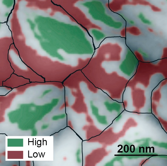
This atomic force microscopy image of the grainy surface of a perovskite solar cell reveals a new path to much greater efficiency. Individual grains are outlined in black, low-performing facets are red, and high-performing facets are green. A big jump in efficiency could possibly be obtained if the material can be grown so that more high-performing facets develop. (Credit: Berkeley Lab)

This atomic force microscopy image of the grainy surface of a perovskite solar cell reveals a new path to much greater efficiency. Individual grains are outlined in black, low-performing facets are red, and high-performing facets are green. A big jump in efficiency could possibly be obtained if the material can be grown so that more high-performing facets develop. (Credit: Berkeley Lab)

It’s always fascinating to observe a trend (or a craze) in science, an endeavour that outsiders (like me) tend to think of as impervious to such vagaries. Perovskite seems to be making its way past the trend/craze phase and moving into a more meaningful phase. From a July 4, 2016 news item on Nanowerk,

Scientists from the Department of Energy’s Lawrence Berkeley National Laboratory (Berkeley Lab) have discovered a possible secret to dramatically boosting the efficiency of perovskite solar cells hidden in the nanoscale peaks and valleys of the crystalline material.

Solar cells made from compounds that have the crystal structure of the mineral perovskite have captured scientists’ imaginations. They’re inexpensive and easy to fabricate, like organic solar cells. Even more intriguing, the efficiency at which perovskite solar cells convert photons to electricity has increased more rapidly than any other material to date, starting at three percent in 2009 — when researchers first began exploring the material’s photovoltaic capabilities — to 22 percent today. This is in the ballpark of the efficiency of silicon solar cells.

Now, as reported online July 4, 2016 in the journal Nature Energy (“Facet-dependent photovoltaic efficiency variations in single grains of hybrid halide perovskite”), a team of scientists from the Molecular Foundry and the Joint Center for Artificial Photosynthesis, both at Berkeley Lab, found a surprising characteristic of a perovskite solar cell that could be exploited for even higher efficiencies, possibly up to 31 percent.

A July 4, 2016 Berkeley Lab news release (also on EurekAlert), which originated the news item, details the research,

Using photoconductive atomic force microscopy, the scientists mapped two properties on the active layer of the solar cell that relate to its photovoltaic efficiency. The maps revealed a bumpy surface composed of grains about 200 nanometers in length, and each grain has multi-angled facets like the faces of a gemstone.

Unexpectedly, the scientists discovered a huge difference in energy conversion efficiency between facets on individual grains. They found poorly performing facets adjacent to highly efficient facets, with some facets approaching the material’s theoretical energy conversion limit of 31 percent.

The scientists say these top-performing facets could hold the secret to highly efficient solar cells, although more research is needed.

“If the material can be synthesized so that only very efficient facets develop, then we could see a big jump in the efficiency of perovskite solar cells, possibly approaching 31 percent,” says Sibel Leblebici, a postdoctoral researcher at the Molecular Foundry.

Leblebici works in the lab of Alexander Weber-Bargioni, who is a corresponding author of the paper that describes this research. Ian Sharp, also a corresponding author, is a Berkeley Lab scientist at the Joint Center for Artificial Photosynthesis. Other Berkeley Lab scientists who contributed include Linn Leppert, Francesca Toma, and Jeff Neaton, the director of the Molecular Foundry.

A team effort

The research started when Leblebici was searching for a new project. “I thought perovskites are the most exciting thing in solar right now, and I really wanted to see how they work at the nanoscale, which has not been widely studied,” she says.

She didn’t have to go far to find the material. For the past two years, scientists at the nearby Joint Center for Artificial Photosynthesis have been making thin films of perovskite-based compounds, and studying their ability to convert sunlight and CO2 into useful chemicals such as fuel. Switching gears, they created pervoskite solar cells composed of methylammonium lead iodide. They also analyzed the cells’ performance at the macroscale.

The scientists also made a second set of half cells that didn’t have an electrode layer. They packed eight of these cells on a thin film measuring one square centimeter. These films were analyzed at the Molecular Foundry, where researchers mapped the cells’ surface topography at a resolution of ten nanometers. They also mapped two properties that relate to the cells’ photovoltaic efficiency: photocurrent generation and open circuit voltage.

This was performed using a state-of-the-art atomic force microscopy technique, developed in collaboration with Park Systems, which utilizes a conductive tip to scan the material’s surface. The method also eliminates friction between the tip and the sample. This is important because the material is so rough and soft that friction can damage the tip and sample, and cause artifacts in the photocurrent.

Surprise discovery could lead to better solar cells

The resulting maps revealed an order of magnitude difference in photocurrent generation, and a 0.6-volt difference in open circuit voltage, between facets on the same grain. In addition, facets with high photocurrent generation had high open circuit voltage, and facets with low photocurrent generation had low open circuit voltage.

“This was a big surprise. It shows, for the first time, that perovskite solar cells exhibit facet-dependent photovoltaic efficiency,” says Weber-Bargioni.

Adds Toma, “These results open the door to exploring new ways to control the development of the material’s facets to dramatically increase efficiency.”

In practice, the facets behave like billions of tiny solar cells, all connected in parallel. As the scientists discovered, some cells operate extremely well and others very poorly. In this scenario, the current flows towards the bad cells, lowering the overall performance of the material. But if the material can be optimized so that only highly efficient facets interface with the electrode, the losses incurred by the poor facets would be eliminated.

“This means, at the macroscale, the material could possibly approach its theoretical energy conversion limit of 31 percent,” says Sharp.

A theoretical model that describes the experimental results predicts these facets should also impact the emission of light when used as an LED. …

The Molecular Foundry is a DOE Office of Science User Facility located at Berkeley Lab. The Joint Center for Artificial Photosynthesis is a DOE Energy Innovation Hub led by the California Institute of Technology in partnership with Berkeley Lab.

Here’s a link to and a citation for the paper,

Facet-dependent photovoltaic efficiency variations in single grains of hybrid halide perovskite by Sibel Y. Leblebici, Linn Leppert, Yanbo Li, Sebastian E. Reyes-Lillo, Sebastian Wickenburg, Ed Wong, Jiye Lee, Mauro Melli, Dominik Ziegler, Daniel K. Angell, D. Frank Ogletree, Paul D. Ashby, Francesca M. Toma, Jeffrey B. Neaton, Ian D. Sharp, & Alexander Weber-Bargioni. Nature Energy 1, Article number: 16093 (2016  doi:10.1038/nenergy.2016.93 Published online: 04 July 2016

This paper is behind a paywall.

Dexter Johnson’s July 6, 2016 posting on his Nanoclast blog (on the IEEE [Institute of Electrical and Electronics Engineers] website} presents his take on the impact that this new finding may have,

The rise of the crystal perovskite as a potential replacement for silicon in photovoltaics has been impressive over the last decade, with its conversion efficiency improving from 3.8 to 22.1 percent over that time period. Nonetheless, there has been a vague sense that this rise is beginning to peter out of late, largely because when a solar cell made from perovskite gets larger than 1 square centimeter the best conversion efficiency had been around 15.6 percent. …

‘Bionic’ cardiac patch with nanoelectric scaffolds and living cells

A June 27, 2016 news item on Nanowerk announced that Harvard University researchers may have taken us a step closer to bionic cardiac patches for human hearts (Note: A link has been removed),

Scientists and doctors in recent decades have made vast leaps in the treatment of cardiac problems – particularly with the development in recent years of so-called “cardiac patches,” swaths of engineered heart tissue that can replace heart muscle damaged during a heart attack.

Thanks to the work of Charles Lieber and others, the next leap may be in sight.

The Mark Hyman, Jr. Professor of Chemistry and Chair of the Department of Chemistry and Chemical Biology, Lieber, postdoctoral fellow Xiaochuan Dai and other co-authors of a study that describes the construction of nanoscale electronic scaffolds that can be seeded with cardiac cells to produce a “bionic” cardiac patch. The study is described in a June 27 [2016] paper published in Nature Nanotechnology (“Three-dimensional mapping and regulation of action potential propagation in nanoelectronics-innervated tissues”).

A June 27, 2016 Harvard University press release on EurekAlert, which originated the news item, provides more information,

“I think one of the biggest impacts would ultimately be in the area that involves replaced of damaged cardiac tissue with pre-formed tissue patches,” Lieber said. “Rather than simply implanting an engineered patch built on a passive scaffold, our works suggests it will be possible to surgically implant an innervated patch that would now be able to monitor and subtly adjust its performance.”

Once implanted, Lieber said, the bionic patch could act similarly to a pacemaker – delivering electrical shocks to correct arrhythmia, but the possibilities don’t end there.

“In this study, we’ve shown we can change the frequency and direction of signal propagation,” he continued. “We believe it could be very important for controlling arrhythmia and other cardiac conditions.”

Unlike traditional pacemakers, Lieber said, the bionic patch – because its electronic components are integrated throughout the tissue – can detect arrhythmia far sooner, and operate at far lower voltages.

“Even before a person started to go into large-scale arrhythmia that frequently causes irreversible damage or other heart problems, this could detect the early-stage instabilities and intervene sooner,” he said. “It can also continuously monitor the feedback from the tissue and actively respond.”

“And a normal pacemaker, because it’s on the surface, has to use relatively high voltages,” Lieber added.

The patch might also find use, Lieber said, as a tool to monitor the responses under cardiac drugs, or to help pharmaceutical companies to screen the effectiveness of drugs under development.

Likewise, the bionic cardiac patch can also be a unique platform, he further mentioned, to study the tissue behavior evolving during some developmental processes, such as aging, ischemia or differentiation of stem cells into mature cardiac cells.

Although the bionic cardiac patch has not yet been implanted in animals, “we are interested in identifying collaborators already investigating cardiac patch implantation to treat myocardial infarction in a rodent model,” he said. “I don’t think it would be difficult to build this into a simpler, easily implantable system.”

In the long term, Lieber believes, the development of nanoscale tissue scaffolds represents a new paradigm for integrating biology with electronics in a virtually seamless way.

Using the injectable electronics technology he pioneered last year, Lieber even suggested that similar cardiac patches might one day simply be delivered by injection.

“It may actually be that, in the future, this won’t be done with a surgical patch,” he said. “We could simply do a co-injection of cells with the mesh, and it assembles itself inside the body, so it’s less invasive.”

Here’s a link to and a citation for the paper,

Three-dimensional mapping and regulation of action potential propagation in nanoelectronics-innervated tissues by Xiaochuan Dai, Wei Zhou, Teng Gao, Jia Liu & Charles M. Lieber. Nature Nanotechnology (2016)  doi:10.1038/nnano.2016.96 Published online 27 June 2016

This paper is behind a paywall.

Dexter Johnson in a June 27, 2016 posting on his Nanoclast blog (on the IEEE [Institute of Electrical and Electronics Engineers] website) provides more technical detail (Note: Links have been removed),

In research described in the journal Nature Nanotechnology, Lieber and his team employed a bottom-up approach that started with the fabrication of doped p-type silicon nanowires. Lieber has been spearheading the use of silicon nanowires as a scaffold for growing nerve, heart, and muscle tissue for years now.

In this latest work, Lieber and his team fabricated the nanowires, applied them onto a polymer surface, and arranged them into a field-effect transistor (FET). The researchers avoided an increase in the device’s impedance as its dimensions were reduced by adopting this FET approach as opposed to simply configuring the device as an electrode. Each FET, along with its source-drain interconnects, created a 4-micrometer-by-20-micrometer-by-350-nanometer pad. Each of these pads was, in effect, a single recording device.

I recommend reading Dexter’s posting in its entirety as Charles Lieber shares additional technical information not found in the news release.

Printing in midair

Dexter Johnson’s May 16, 2016 posting on his Nanoclast blog (on the IEEE [Institute of Electrical and Electronics Engineers] website) was my first introduction to something wonder-inducing (Note: Links have been removed),

While the growth of 3-D printing has led us to believe we can produce just about any structure with it, the truth is that it still falls somewhat short.

Researchers at Harvard University are looking to realize a more complete range of capabilities for 3-D printing in fabricating both planar and freestanding 3-D structures and do it relatively quickly and on low-cost plastic substrates.

In research published in the journal Proceedings of the National Academy of Sciences (PNAS),  the researchers extruded a silver-nanoparticle ink and annealed it with a laser so quickly that the system let them easily “write” free-standing 3-D structures.

While this may sound humdrum, what really takes one’s breath away with this technique is that it can create 3-D structures seemingly suspended in air without any signs of support as though they were drawn there with a pen.

Laser-assisted direct ink writing allowed this delicate 3D butterfly to be printed without any auxiliary support structure (Image courtesy of the Lewis Lab/Harvard University)

Laser-assisted direct ink writing allowed this delicate 3D butterfly to be printed without any auxiliary support structure (Image courtesy of the Lewis Lab/Harvard University)

A May 16, 2016 Harvard University press release (also on EurekAlert) provides more detail about the work,

“Flat” and “rigid” are terms typically used to describe electronic devices. But the increasing demand for flexible, wearable electronics, sensors, antennas and biomedical devices has led a team at Harvard’s John A. Paulson School of Engineering and Applied Sciences (SEAS) and Wyss Institute for Biologically Inspired Engineering to innovate an eye-popping new way of printing complex metallic architectures – as though they are seemingly suspended in midair.

“I am truly excited by this latest advance from our lab, which allows one to 3D print and anneal flexible metal electrodes and complex architectures ‘on-the-fly,’ ” said Lewis [Jennifer Lewis, the Hansjörg Wyss Professor of Biologically Inspired Engineering at SEAS and Wyss Core Faculty member].

Lewis’ team used an ink composed of silver nanoparticles, sending it through a printing nozzle and then annealing it using a precisely programmed laser that applies just the right amount of energy to drive the ink’s solidification. The printing nozzle moves along x, y, and z axes and is combined with a rotary print stage to enable freeform curvature. In this way, tiny hemispherical shapes, spiral motifs, even a butterfly made of silver wires less than the width of a hair can be printed in free space within seconds. The printed wires exhibit excellent electrical conductivity, almost matching that of bulk silver.

When compared to conventional 3D printing techniques used to fabricate conductive metallic features, laser-assisted direct ink writing is not only superior in its ability to produce curvilinear, complex wire patterns in one step, but also in the sense that localized laser heating enables electrically conductive silver wires to be printed directly on low-cost plastic substrates.

According to the study’s first author, Wyss Institute Postdoctoral Fellow Mark Skylar-Scott, Ph.D., the most challenging aspect of honing the technique was optimizing the nozzle-to-laser separation distance.

“If the laser gets too close to the nozzle during printing, heat is conducted upstream which clogs the nozzle with solidified ink,” said Skylar-Scott. “To address this, we devised a heat transfer model to account for temperature distribution along a given silver wire pattern, allowing us to modulate the printing speed and distance between the nozzle and laser to elegantly control the laser annealing process ‘on the fly.’ ”

The result is that the method can produce not only sweeping curves and spirals but also sharp angular turns and directional changes written into thin air with silver inks, opening up near limitless new potential applications in electronic and biomedical devices that rely on customized metallic architectures.

Seeing is believing, eh?

Here’s a link to and a citation for the paper,

Laser-assisted direct ink writing of planar and 3D metal architectures by Mark A. Skylar-Scott, Suman Gunasekaran, and Jennifer A. Lewis. PNAS [Proceedings of the National Academy of Sciences] 2016 doi: 10.1073/pnas.1525131113

I believe this paper is open access.

A question: I wonder what conditions are necessary before you can 3D print something in midair? Much as I’m dying to try this at home, I’m pretty that’s not possible.

2-D boron as a superconductor

A March 31, 2016 news item on ScienceDaily highlights some research into 2D (two-dimensional) boron at Rice University (Texas, US),

Rice University scientists have determined that two-dimensional boron is a natural low-temperature superconductor. In fact, it may be the only 2-D material with such potential.

Rice theoretical physicist Boris Yakobson and his co-workers published their calculations that show atomically flat boron is metallic and will transmit electrons with no resistance. …

The hitch, as with most superconducting materials, is that it loses its resistivity only when very cold, in this case between 10 and 20 kelvins (roughly, minus-430 degrees Fahrenheit). But for making very small superconducting circuits, it might be the only game in town.

A March 30, 2016 Rice University news release (also on EurekAlert but dated March 31, 2016), which originated the news item, expands on the theme,

The basic phenomenon of superconductivity has been known for more than 100 years, said Evgeni Penev, a research scientist in the Yakobson group, but had not been tested for its presence in atomically flat boron.

“It’s well-known that the material is pretty light because the atomic mass is small,” Penev said. “If it’s metallic too, these are two major prerequisites for superconductivity. That means at low temperatures, electrons can pair up in a kind of dance in the crystal.”

“Lower dimensionality is also helpful,” Yakobson said. “It may be the only, or one of very few, two-dimensional metals. So there are three factors that gave the initial motivation for us to pursue the research. Then we just got more and more excited as we got into it.”

Electrons with opposite momenta and spins effectively become Cooper pairs; they attract each other at low temperatures with the help of lattice vibrations, the so-called “phonons,” and give the material its superconducting properties, Penev said. “Superconductivity becomes a manifestation of the macroscopic wave function that describes the whole sample. It’s an amazing phenomenon,” he said.

It wasn’t entirely by chance that the first theoretical paper establishing conductivity in a 2-D material appeared at roughly the same time the first samples of the material were made by laboratories in the United States and China. In fact, an earlier paper by the Yakobson group had offered a road map for doing so.

That 2-D boron has now been produced is a good thing, according to Yakobson and lead authors Penev and Alex Kutana, a postdoctoral researcher at Rice. “We’ve been working to characterize boron for years, from cage clusters to nanotubes to planer sheets, but the fact that these papers appeared so close together means these labs can now test our theories,” Yakobson said.

“In principle, this work could have been done three years ago as well,” he said. “So why didn’t we? Because the material remained hypothetical; okay, theoretically possible, but we didn’t have a good reason to carry it too far.

“But then last fall it became clear from professional meetings and interactions that it can be made. Now those papers are published. When you think it’s coming for real, the next level of exploration becomes more justifiable,” Yakobson said.

Boron atoms can make more than one pattern when coming together as a 2-D material, another characteristic predicted by Yakobson and his team that has now come to fruition. These patterns, known as polymorphs, may allow researchers to tune the material’s conductivity “just by picking a selective arrangement of the hexagonal holes,” Penev said.

He also noted boron’s qualities were hinted at when researchers discovered more than a decade ago that magnesium diborite is a high-temperature electron-phonon superconductor. “People realized a long time ago the superconductivity is due to the boron layer,” Penev said. “The magnesium acts to dope the material by spilling some electrons into the boron layer. In this case, we don’t need them because the 2-D boron is already metallic.”

Penev suggested that isolating 2-D boron between layers of inert hexagonal boron nitride (aka “white graphene”) might help stabilize its superconducting nature.

Without the availability of a block of time on several large government supercomputers, the study would have taken a lot longer, Yakobson said. “Alex did the heavy lifting on the computational work,” he said. “To turn it from a lunchtime discussion into a real quantitative research result took a very big effort.”

The paper is the first by Yakobson’s group on the topic of superconductivity, though Penev is a published author on the subject. “I started working on superconductivity in 1993, but it was always kind of a hobby, and I hadn’t done anything on the topic in 10 years,” Penev said. “So this paper brings it full circle.”

Here’s a link to and a citation for the paper,

Can Two-Dimensional Boron Superconduct? by Evgeni S. Penev, Alex Kutana, and Boris I. Yakobson. Nano Lett., Article ASAP DOI: 10.1021/acs.nanolett.6b00070 Publication Date (Web): March 22, 2016

Copyright © 2016 American Chemical Society

This paper is behind a paywall.

Dexter Johnson has published an April 5, 2016 post on his Nanoclast blog (on the IEEE [Institute of Electrical and Electronics Engineers] website) about this latest Rice University work on 2D boron that includes comments from his email interview with Penev.