Tag Archives: University of Manchester

World’s first ever graphene-enhanced sports shoes/sneakers/running shoes/runners/trainers

Regardless of what these shoes are called, they contain, apparently, some graphene. As to why you as a consumer might find that important, here’s more from a June 20, 2018 news item on Nanowerk,

The world’s first-ever sports shoes to utilise graphene – the strongest material on the planet – have been unveiled by The University of Manchester and British brand inov-8.

Collaborating with graphene experts at National Graphene Institute, the brand has been able to develop a graphene-enhanced rubber. They have developed rubber outsoles for running and fitness shoes that in testing have outlasted 1,000 miles and are scientifically proven to be 50% harder wearing.

The National Graphene Institute (located at the UK’s University of Manchester) June 20, 2018 press release, which originated the news item, provides a few details, none of them particularly technical or scientific, no mention of studies, etc.  (Note: Links have been removed),

Graphene is 200 times stronger than steel and at only a single atom thick it is the thinnest possible material, meaning it has many unique properties. inov-8 is the first brand in the world to use the superlative material in sports footwear, with its G-SERIES shoes available to pre-order from June 22nd [2018] ahead of going on sale from July 12th [2018].

The company first announced its intent to revolutionise the sports footwear industry in December last year. Six months of frenzied anticipation later, inov-8 has now removed all secrecy and let the world see these game-changing shoes.

Michael Price, inov-8 product and marketing director, said: “Over the last 18 months we have worked with the National Graphene Institute at The University of Manchester to bring the world’s toughest grip to the sports footwear market.

“Prior to this innovation, off-road runners and fitness athletes had to choose between a sticky rubber that works well in wet or sweaty conditions but wears down quicker and a harder rubber that is more durable but not quite as grippy. Through intensive research, hundreds of prototypes and thousands of hours of testing in both the field and laboratory, athletes now no longer need to compromise.”

Dr Aravind Vijayaraghavan, Reader in Nanomaterials at The University of Manchester, said: “Using graphene we have developed G-SERIES outsole rubbers that are scientifically tested to be 50% stronger, 50% more elastic and 50% harder wearing.

“We are delighted to put graphene on the shelves of 250 retail stores all over the world and make it accessible to everyone. Graphene is a versatile material with limitless potential and in coming years we expect to deliver graphene technologies in composites, coatings and sensors, many of which will further revolutionise sports products.”

The G-SERIES range is made up of three different shoes, each meticulously designed to meet the needs of athletes. THE MUDCLAW G 260 is for running over muddy mountains and obstacle courses, the TERRAULTRA G 260 for running long distances on hard-packed trails and the F-LITE G 290 for crossfitters working out in gyms. Each includes graphene-enhanced rubber outsoles and Kevlar – a material used in bulletproof vests – on the uppers.

Commenting on the patent-pending technology and the collaboration with The University of Manchester, inov-8 CEO Ian Bailey said: “This powerhouse forged in Northern England is going to take the world of sports footwear by storm. We’re combining science and innovation together with entrepreneurial speed and agility to go up against the major sports brands – and we’re going to win.

“We are at the forefront of a graphene sports footwear revolution and we’re not stopping at just rubber outsoles. This is a four-year innovation project which will see us incorporate graphene into 50% of our range and give us the potential to halve the weight of running/fitness shoes without compromising on performance or durability.”

Graphene is produced from graphite, which was first mined in the Lake District fells of Northern England more than 450 years ago. inov-8 too was forged in the same fells, albeit much more recently in 2003. The brand now trades in 68 countries worldwide.

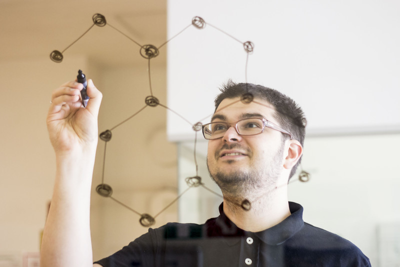
The scientists who first isolated graphene from graphite were awarded the Nobel Prize in 2010. Building on their revolutionary work, a team of over 300 staff at The University of Manchester has pioneered projects into graphene-enhanced prototypes, from sports cars and medical devices to aeroplanes. Now the University can add graphene-enhanced sports footwear to its list of world-firsts.

A picture of the ‘shoes’ has been provided,

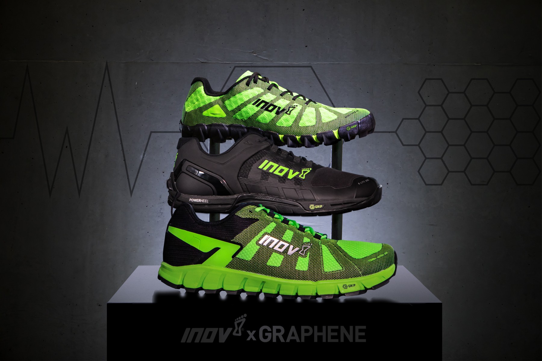
Courtesy: National Graphene Institute at University of Manchester

You can find the company inov-8 here. As for more information about their graphene-enhanced show, there’s this,from the company’s ‘graphene webpage‘,

1555Graphite was first mined in the Lake District fells of Northern England

2004Scientists at The University of Manchester isolate graphene from graphite.

2010The Nobel Prize is awarded to the scientists for their ground-breaking experiments with graphene.

2018inov-8 launch the first-ever sports footwear to utilise graphene, delivering the world’s toughest grip.

Ground-breaking technology

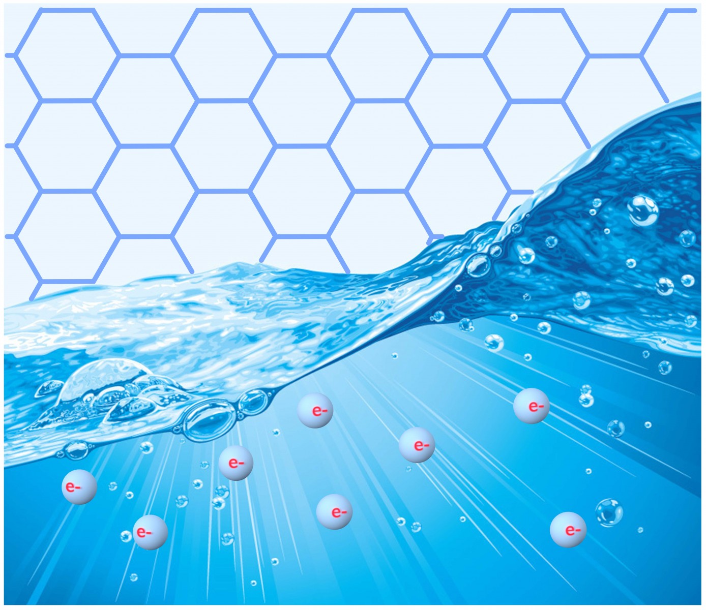
One atom thick carbon sheet

200 x stronger than steel

Thin, light, flexible, with limitless potential

inov-8 COLLABORATION WITH THE NATIONAL GRAPHENE INSTITUTE

Previously athletes had to choose between a sticky rubber that works well in wet or sweaty conditions but wears down quicker, and a harder rubber that is more durable but not quite as grippy. Through intensive research, hundreds of prototypes and thousands of hours of testing in both the field and laboratory, athletes now no longer need to compromise. The new rubber we have developed with the National Graphene Institute at The University of Manchester allows us to smash the limits of grip [sic]

The G-SERIES range is made up of three different shoes, each meticulously designed to meet the needs of athletes. Each includes graphene-enhanced rubber outsoles that deliver the world’s toughest grip and Kevlar – a material used in bulletproof vests – on the uppers.

Bulletproof material for running shoes?

As for Canadians eager to try out these shoes, you will likely have to go online or go to the US.  Given how recently (June 19, 2018) this occurred, I’m mentioning the US president’s (Donald Trump) comments that Canadians are notorious for buying shoes in the US and smuggling them across the border back into Canada. (Revelatory information for Canadians everywhere.) His bizarre comments occasioned this explanatory June 19, 2018 article by Jordan Weissmann for Slate.com,

During a characteristically rambling address before the National Federation of Independent Businesses on Tuesday [June 19, 2018], Donald Trump darted off into an odd tangent in which he suggested that Canadians were smuggling shoes across the U.S. border in order to avoid their country’s high tariffs.

There was a story two days ago in a major newspaper talking about people living in Canada coming into the United States and smuggling things back into Canada because the tariffs are so massive. The tariffs to get common items back into Canada are so high that they have to smuggle ‘em in. They buy shoes, then they wear ‘em. They scuff ‘em up. They make ‘em sound old or look old. No, we’re treated horribly. [emphasis mine]

Anyone engaged in this alleged practice would be avoiding payment to the Canadian government. How this constitutes poor treatment of the US government and/or US retailers is a bit a of puzzler.

Getting back to Weissman and his article, he focuses on the source of the US president’s ‘information’.

As for graphene-enhanced ‘shoes’, I hope they are as advertized.

Socially responsible AI—it’s time says University of Manchester (UK) researchers

A May 10, 2018 news item on ScienceDaily describes a report on the ‘fourth industrial revolution’ being released by the University of Manchester,

The development of new Artificial Intelligence (AI) technology is often subject to bias, and the resulting systems can be discriminatory, meaning more should be done by policymakers to ensure its development is democratic and socially responsible.

This is according to Dr Barbara Ribeiro of Manchester Institute of Innovation Research at The University of Manchester, in On AI and Robotics: Developing policy for the Fourth Industrial Revolution, a new policy report on the role of AI and Robotics in society, being published today [May 10, 2018].

Interestingly, the US White House is hosting a summit on AI today, May 10, 2018, according to a May 8, 2018 article by Danny Crichton for TechCrunch (Note: Links have been removed),

Now, it appears the White House itself is getting involved in bringing together key American stakeholders to discuss AI and those opportunities and challenges. …

Among the confirmed guests are Facebook’s Jerome Pesenti, Amazon’s Rohit Prasad, and Intel’s CEO Brian Krzanich. While the event has many tech companies present, a total of 38 companies are expected to be in attendance including United Airlines and Ford.

AI policy has been top-of-mind for many policymakers around the world. French President Emmanuel Macron has announced a comprehensive national AI strategy, as has Canada, which has put together a research fund and a set of programs to attempt to build on the success of notable local AI researchers such as University of Toronto professor George Hinton, who is a major figure in deep learning.

But it is China that has increasingly drawn the attention and concern of U.S. policymakers. The country and its venture capitalists are outlaying billions of dollars to invest in the AI industry, and it has made leading in artificial intelligence one of the nation’s top priorities through its Made in China 2025 program and other reports. …

In comparison, the United States has been remarkably uncoordinated when it comes to AI. …

That lack of engagement from policymakers has been fine — after all, the United States is the world leader in AI research. But with other nations pouring resources and talent into the space, DC policymakers are worried that the U.S. could suddenly find itself behind the frontier of research in the space, with particular repercussions for the defense industry.

Interesting contrast: do we take time to consider the implications or do we engage in a race?

While it’s becoming fashionable to dismiss dichotomous questions of this nature, the two approaches (competition and reflection) are not that compatible and it does seem to be an either/or proposition.

A May 10, 2018 University of Manchester press release (also on EurekAlert), which originated the news item, expands on the theme of responsibility and AI,

Dr Ribeiro adds because investment into AI will essentially be paid for by tax-payers in the long-term, policymakers need to make sure that the benefits of such technologies are fairly distributed throughout society.

She says: “Ensuring social justice in AI development is essential. AI technologies rely on big data and the use of algorithms, which influence decision-making in public life and on matters such as social welfare, public safety and urban planning.”

“In these ‘data-driven’ decision-making processes some social groups may be excluded, either because they lack access to devices necessary to participate or because the selected datasets do not consider the needs, preferences and interests of marginalised and disadvantaged people.”

On AI and Robotics: Developing policy for the Fourth Industrial Revolution is a comprehensive report written, developed and published by Policy@Manchester with leading experts and academics from across the University.

The publication is designed to help employers, regulators and policymakers understand the potential effects of AI in areas such as industry, healthcare, research and international policy.

However, the report doesn’t just focus on AI. It also looks at robotics, explaining the differences and similarities between the two separate areas of research and development (R&D) and the challenges policymakers face with each.

Professor Anna Scaife, Co-Director of the University’s Policy@Manchester team, explains: “Although the challenges that companies and policymakers are facing with respect to AI and robotic systems are similar in many ways, these are two entirely separate technologies – something which is often misunderstood, not just by the general public, but policymakers and employers too. This is something that has to be addressed.”

One particular area the report highlights where robotics can have a positive impact is in the world of hazardous working environments, such a nuclear decommissioning and clean-up.

Professor Barry Lennox, Professor of Applied Control and Head of the UOM Robotics Group, adds: “The transfer of robotics technology into industry, and in particular the nuclear industry, requires cultural and societal changes as well as technological advances.

“It is really important that regulators are aware of what robotic technology is and is not capable of doing today, as well as understanding what the technology might be capable of doing over the next -5 years.”

The report also highlights the importance of big data and AI in healthcare, for example in the fight against antimicrobial resistance (AMR).

Lord Jim O’Neill, Honorary Professor of Economics at The University of Manchester and Chair of the Review on Antimicrobial Resistance explains: “An important example of this is the international effort to limit the spread of antimicrobial resistance (AMR). The AMR Review gave 27 specific recommendations covering 10 broad areas, which became known as the ‘10 Commandments’.

“All 10 are necessary, and none are sufficient on their own, but if there is one that I find myself increasingly believing is a permanent game-changer, it is state of the art diagnostics. We need a ‘Google for doctors’ to reduce the rate of over prescription.”

The versatile nature of AI and robotics is leading many experts to predict that the technologies will have a significant impact on a wide variety of fields in the coming years. Policy@Manchester hopes that the On AI and Robotics report will contribute to helping policymakers, industry stakeholders and regulators better understand the range of issues they will face as the technologies play ever greater roles in our everyday lives.

As far as I can tell, the report has been designed for online viewing only. There are none of the markers (imprint date, publisher, etc.) that I expect to see on a print document. There is no bibliography or list of references but there are links to outside sources throughout the document.

It’s an interesting approach to publishing a report that calls for social justice, especially since the issue of ‘trust’ is increasingly being emphasized where all AI is concerned. With regard to this report, I’m not sure I can trust it. With a print document or a PDF I have markers. I can examine the index, the bibliography, etc. and determine if this material has covered the subject area with reference to well known authorities. It’s much harder to do that with this report. As well, this ‘souped up’ document also looks like it might be easy to change something without my knowledge. With a print or PDF version, I can compare the documents but not with this one.

Nanobots—at last

Who can resist Etta James? Getting to the point of the post, I’ve been reading about nanobots for years but this is the first time I’ve seen something that resembles what lived in my imagination—at last. From a Sept. 20 , 2017 news item on phys.org (Note: Links have been removed),

Scientists at The University of Manchester have created the world’s first ‘molecular robot’ that is capable of performing basic tasks including building other molecules.

The tiny robots, which are a millionth of a millimetre in size, can be programmed to move and build molecular cargo, using a tiny robotic arm.

Each individual robot is capable of manipulating a single molecule and is made up of just 150 carbon, hydrogen, oxygen and nitrogen atoms. To put that size into context, a billion billion of these robots piled on top of each other would still only be the same size as a single grain of salt.

The robots operate by carrying out chemical reactions in special solutions which can then be controlled and programmed by scientists to perform the basic tasks.

In the future such robots could be used for medical purposes, advanced manufacturing processes and even building molecular factories and assembly lines. …

A Sept. 20, 2017 University of Manchester press release (also on EurekAlert), which originated the news item, provides (perhaps) a little more explanation than is absolutely necessary,

Professor David Leigh, who led the research at University’s School of Chemistry, explains: ‘All matter is made up of atoms and these are the basic building blocks that form molecules. [emphasis mine] Our robot is literally a molecular robot constructed of atoms just like you can build a very simple robot out of Lego bricks. The robot then responds to a series of simple commands that are programmed with chemical inputs by a scientist.

‘It is similar to the way robots are used on a car assembly line. Those robots pick up a panel and position it so that it can be riveted in the correct way to build the bodywork of a car. So, just like the robot in the factory, our molecular version can be programmed to position and rivet components in different ways to build different products, just on a much smaller scale at a molecular level.’

The benefit of having machinery that is so small is it massively reduces demand for materials, can accelerate and improve drug discovery, dramatically reduce power requirements and rapidly increase the miniaturisation of other products. Therefore, the potential applications for molecular robots are extremely varied and exciting.

Prof Leigh says: ‘Molecular robotics represents the ultimate in the miniaturisation of machinery. Our aim is to design and make the smallest machines possible. This is just the start but we anticipate that within 10 to 20 years molecular robots will begin to be used to build molecules and materials on assembly lines in molecular factories.’

Whilst building and operating such tiny machine is extremely complex, the techniques used by the team are based on simple chemical processes.

Prof Leigh added: ‘The robots are assembled and operated using chemistry. This is the science of how atoms and molecules react with each other and how larger molecules are constructed from smaller ones.

‘It is the same sort of process scientists use to make medicines and plastics from simple chemical building blocks. Then, once the nano-robots have been constructed, they are operated by scientists by adding chemical inputs which tell the robots what to do and when, just like a computer program.’

Here’s a link to and a citation for the paper,

Stereodivergent synthesis with a programmable molecular machine by Salma Kassem, Alan T. L. Lee, David A. Leigh, Vanesa Marcos, Leoni I. Palmer, & Simone Pisano. Nature 549,
374–378 (21 September 2017) doi:10.1038/nature23677 Published online 20 September 2017

This paper is behind a paywall.

There’s a rather attractive image accompanying the news release which manages to be both quite informative and wholly unrealistic,

Courtesy: University of Manchester

Nanobots first made their way into popular science with K. Eric Drexler’s book 1986, Engines of Creation, which also provoked a spirited academic debate. See Drexler’s Wikipedia entry for more. One final comment, this would seem to be a promising start to the long-held dream of bottom-up engineering of materials.

A new wave of physics: electrons flow like liquid in graphene

Unfortunately I couldn’t find a credit for the artist for the graphic (I really like it) which accompanies the news about a new physics and graphene,

Courtesy: University of Manchester

From an Aug. 22, 2017 news item on phys.org (Note: A link has been removed),

A new understanding of the physics of conductive materials has been uncovered by scientists observing the unusual movement of electrons in graphene.

Graphene is many times more conductive than copper thanks, in part, to its two-dimensional structure. In most metals, conductivity is limited by crystal imperfections which cause electrons to frequently scatter like billiard balls when they move through the material.

Now, observations in experiments at the National Graphene Institute have provided essential understanding as to the peculiar behaviour of electron flows in graphene, which need to be considered in the design of future Nano-electronic circuits.

An Aug. 22, 2017 University of Manchester press release, which originated the news item, delves further into the research (Note: Links have been removed),

Appearing today in Nature Physics, researchers at The University of Manchester, in collaboration with theoretical physicists led by Professor Marco Polini and Professor Leonid Levitov, show that Landauer’s fundamental limit can be breached in graphene. Even more fascinating is the mechanism responsible for this.

Last year, a new field in solid-state physics termed ‘electron hydrodynamics’ generated huge scientific interest. Three different experiments, including one performed by The University of Manchester, demonstrated that at certain temperatures, electrons collide with each other so frequently they start to flow collectively like a viscous fluid.

The new research demonstrates that this viscous fluid is even more conductive than ballistic electrons. The result is rather counter-intuitive, since typically scattering events act to lower the conductivity of a material, because they inhibit movement within the crystal. However, when electrons collide with each other, they start working together and ease current flow.

This happens because some electrons remain near the crystal edges, where momentum dissipation is highest, and move rather slowly. At the same time, they protect neighbouring electrons from colliding with those regions. Consequently, some electrons become super-ballistic as they are guided through the channel by their friends.

Sir Andre Geim said: “We know from school that additional disorder always creates extra electrical resistance. In our case, disorder induced by electron scattering actually reduces rather than increase resistance. This is unique and quite counterintuitive: Electrons when make up a liquid start propagating faster than if they were free, like in vacuum”.

The researchers measured the resistance of graphene constrictions, and found it decreases upon increasing temperature, in contrast to the usual metallic behaviour expected for doped graphene.

By studying how the resistance across the constrictions changes with temperature, the scientists revealed a new physical quantity which they called the viscous conductance. The measurements allowed them to determine electron viscosity to such a high precision that the extracted values showed remarkable quantitative agreement with theory.

Here’s a link to and a citation for the paper,

Superballistic flow of viscous electron fluid through graphene constrictions by R. Krishna Kumar, D. A. Bandurin, F. M. D. Pellegrino, Y. Cao, A. Principi, H. Guo, G. H. Auton, M. Ben Shalom, L. A. Ponomarenko, G. Falkovich, K. Watanabe, T. Taniguchi, I. V. Grigorieva, L. S. Levitov, M. Polini, & A. K. Geim. Nature Physics (2017) doi:10.1038/nphys4240 Published online 21 August 2017

This paper is behind a paywall.

Job posting: G20 Water Technologies is looking for a PhD level scientist to join a fast-growing and well-funded start-up company developing graphene based water treatment.

This is the June 6, 2017 G20 Water Technologies notice I received via email,

Senior Application Scientist Vacancy

This is an opportunity for a PhD level scientist to join a fast growing
and well funded start up developing graphene based water treatment.

The company has developed coatings for existing filter materials with
applications in oil/water separation, waste water treatment, dehydration
of organic liquids and desalination, with addressable markets in excess
of £2.8Bn.

We have a vacancy for an exceptional individual with an in depth
understanding of membranes and 2D materials to join our team as a Senior
Application Scientist. This post carries a high degree of responsibility
to deliver results, a salary to match, will report directly to the
company’s CEO and will be based with the Water@Leeds interdisciplinary
group in the University of Leeds.

Key responsibilities include:

* Managing the company’s internal and external research and
development activities with both academic and commercial partners;
* To further develop graphene oxide (GO)-based coatings/membranes for
highly efficient water purification. This will involve working closely
with materials suppliers and end users to understand and deliver the
required performance;
* Developing test methodologies to quantify membrane performance
* Supporting current and future government funded grant work;
* Further developing and strengthening G2O’s IP portfolio.

The successful candidate will be expected to have:

* The ability to design, manage and deliver technology R&D projects;
* Experience in working with academic institutions in an industrial
environment;
* An in depth knowledge of formulation of 2D material dispersions;
* A PhD or other suitable academic qualifications to be accepted as a
Visiting Fellow by the company’s academic partners.

Before getting to the contact information, a few words about one of the company’s principles, Tim Harper, G20 Chief Executive Officer. I’ve never met him in person but have known him online for many years (we’ve exchanged emails and tweets). He has been an active member of the ‘nano’ blogosphere and social media environment for many years. He has run his own consultation company (on emerging technologies), Cientifica (About Us) since 1997, and other companies. He’s been involved with the World Economic Forum and has consulted internationally for governments and other entities. That said, there are no guarantees with start-up companies and you do need to perform your own due diligence as I’m sure Tim Harper would counsel you. One other piece of information before you dash off, the company’s headquarters are in Manchester where its university boasts it’s the ‘home of graphene’ and houses the National Graphene Institute.

Here are a few places you might want to check:

G20 website

About G20 webpage

Contact us (for more details about the position)

Good Luck!

Desalination of sea water with a graphene sieve

The proposed use of graphene membranes for water purification and remediation isn’t new (I have a July 20, 2015 posting which covers some of this field of interest). However, there’s this April 3, 2017 news item on ScienceDaily announcing some new work on graphene and desalination at the University of Manchester,

Graphene-oxide membranes have attracted considerable attention as promising candidates for new filtration technologies. Now the much sought-after development of making membranes capable of sieving common salts has been achieved.

New research demonstrates the real-world potential of providing clean drinking water for millions of people who struggle to access adequate clean water sources.

The new findings from a group of scientists at The University of Manchester were published today in the journal Nature Nanotechnology. Previously graphene-oxide membranes have shown exciting potential for gas separation and water filtration.

An April 3, 2017 University of Manchester press release (also on EurekAlert), which originated the news item, expands on the theme,

Graphene-oxide membranes developed at the National Graphene Institute have already demonstrated the potential of filtering out small nanoparticles, organic molecules, and even large salts. Until now, however, they couldn’t be used for sieving common salts used in desalination technologies, which require even smaller sieves.

Previous research at The University of Manchester found that if immersed in water, graphene-oxide membranes become slightly swollen and smaller salts flow through the membrane along with water, but larger ions or molecules are blocked.

The Manchester-based group have now further developed these graphene membranes and found a strategy to avoid the swelling of the membrane when exposed to water. The pore size in the membrane can be precisely controlled which can sieve common salts out of salty water and make it safe to drink.

As the effects of climate change continue to reduce modern city’s water supplies, wealthy modern countries are also investing in desalination technologies. Following the severe floods in California major wealthy cities are also looking increasingly to alternative water solutions.

When the common salts are dissolved in water, they always form a ‘shell’ of water molecules around the salts molecules. This allows the tiny capillaries of the graphene-oxide membranes to block the salt from flowing along with the water. Water molecules are able to pass through the membrane barrier and flow anomalously fast which is ideal for application of these membranes for desalination.

Professor Rahul Nair, at The University of Manchester said: “Realisation of scalable membranes with uniform pore size down to atomic scale is a significant step forward and will open new possibilities for improving the efficiency of desalination technology.

“This is the first clear-cut experiment in this regime. We also demonstrate that there are realistic possibilities to scale up the described approach and mass produce graphene-based membranes with required sieve sizes.”

Mr. Jijo Abraham and Dr. Vasu Siddeswara Kalangi were the joint-lead authors on the research paper: “The developed membranes are not only useful for desalination, but the atomic scale tunability of the pore size also opens new opportunity to fabricate membranes with on-demand filtration capable of filtering out ions according to their sizes.” said Mr. Abraham.

By 2025 the UN expects that 14% of the world’s population will encounter water scarcity. This technology has the potential to revolutionise water filtration across the world, in particular in countries which cannot afford large scale desalination plants.

It is hoped that graphene-oxide membrane systems can be built on smaller scales making this technology accessible to countries which do not have the financial infrastructure to fund large plants without compromising the yield of fresh water produced.

Courtesy of the University of Manchester

I believe the previous image is an artist’s rendering of the graphene-oxide membrane trapping salt as water moves through it.

Here’s a link to and a citation for the paper,

Tunable sieving of ions using graphene oxide membranes by Jijo Abraham, Kalangi S. Vasu, Christopher D. Williams, Kalon Gopinadhan, Yang Su, Christie T. Cherian, James Dix, Eric Prestat, Sarah J. Haigh, Irina V. Grigorieva, Paola Carbone, Andre K. Geim, & Rahul R. Nair. Nature Nanotechnology (2017) doi:10.1038/nnano.2017.21 Published online 03 April 2017

This paper is open access provided you sign up (or have already signed up) for a free registration with nature.com.

Graphene and silly putty combined to create ultra sensitive sensors

One of my favourite kinds of science story is the one where scientists turn to a children’s toy for their research. In this case, it’s silly putty. Before launching into the science part of this story, here’s more about silly putty from its Wikipedia entry (Note: A ll links have been removed),

During World War II, Japan invaded rubber-producing countries as they expanded their sphere of influence in the Pacific Rim. Rubber was vital for the production of rafts, tires, vehicle and aircraft parts, gas masks, and boots. In the U.S., all rubber products were rationed; citizens were encouraged to make their rubber products last until the end of the war and to donate spare tires, boots, and coats. Meanwhile, the government funded research into synthetic rubber compounds to attempt to solve this shortage.[10]

Credit for the invention of Silly Putty is disputed[11] and has been attributed variously to Earl Warrick,[12] of the then newly formed Dow Corning; Harvey Chin; and James Wright, a Scottish-born inventor working for General Electric in New Haven, Connecticut.[13] Throughout his life, Warrick insisted that he and his colleague, Rob Roy McGregor, received the patent for Silly Putty before Wright did; but Crayola’s history of Silly Putty states that Wright first invented it in 1943.[10][14][15] Both researchers independently discovered that reacting boric acid with silicone oil would produce a gooey, bouncy material with several unique properties. The non-toxic putty would bounce when dropped, could stretch farther than regular rubber, would not go moldy, and had a very high melting temperature. However, the substance did not have all the properties needed to replace rubber.[1]

In 1949 toy store owner Ruth Fallgatter came across the putty. She contacted marketing consultant Peter C.L. Hodgson (1912-1976).[16] The two decided to market the bouncing putty by selling it in a clear case. Although it sold well, Fallgatter did not pursue it further. However, Hodgson saw its potential.[1][3]

Already US$12,000 in debt, Hodgson borrowed US$147 to buy a batch of the putty to pack 1 oz (28 g) portions into plastic eggs for US$1, calling it Silly Putty. Initially, sales were poor, but after a New Yorker article mentioned it, Hodgson sold over 250,000 eggs of silly putty in three days.[3] However, Hodgson was almost put out of business in 1951 by the Korean War. Silicone, the main ingredient in silly putty, was put on ration, harming his business. A year later the restriction on silicone was lifted and the production of Silly Putty resumed.[17][9] Initially, it was primarily targeted towards adults. However, by 1955 the majority of its customers were aged 6 to 12. In 1957, Hodgson produced the first televised commercial for Silly Putty, which aired during the Howdy Doody Show.[18]

In 1961 Silly Putty went worldwide, becoming a hit in the Soviet Union and Europe. In 1968 it was taken into lunar orbit by the Apollo 8 astronauts.[17]

Peter Hodgson died in 1976. A year later, Binney & Smith, the makers of Crayola products, acquired the rights to Silly Putty. As of 2005, annual Silly Putty sales exceeded six million eggs.[19]

Silly Putty was inducted into the National Toy Hall of Fame on May 28, 2001. [20]

I had no idea silly putty had its origins in World War II era research. At any rate, it’s made its way back to the research lab to be united with graphene according to a Dec. 8, 2016 news item  on Nanowerk,

Researchers in AMBER, the Science Foundation Ireland-funded materials science research centre, hosted in Trinity College Dublin, have used graphene to make the novelty children’s material silly putty® (polysilicone) conduct electricity, creating extremely sensitive sensors. This world first research, led by Professor Jonathan Coleman from TCD and in collaboration with Prof Robert Young of the University of Manchester, potentially offers exciting possibilities for applications in new, inexpensive devices and diagnostics in medicine and other sectors.

A Dec. 9, 2016 Trinity College Dublin press release (also on EurekAlert), which originated the news item, describes their ‘G-putty’ in more detail,

Prof Coleman, Investigator in AMBER and Trinity’s School of Physics along with postdoctoral researcher Conor Boland, discovered that the electrical resistance of putty infused with graphene (“G-putty”) was extremely sensitive to the slightest deformation or impact. They mounted the G-putty onto the chest and neck of human subjects and used it to measure breathing, pulse and even blood pressure. It showed unprecedented sensitivity as a sensor for strain and pressure, hundreds of times more sensitive than normal sensors. The G-putty also works as a very sensitive impact sensor, able to detect the footsteps of small spiders. It is believed that this material will find applications in a range of medical devices.

Prof Coleman said, “What we are excited about is the unexpected behaviour we found when we added graphene to the polymer, a cross-linked polysilicone. This material as well known as the children’s toy silly putty. It is different from familiar materials in that it flows like a viscous liquid when deformed slowly but bounces like an elastic solid when thrown against a surface. When we added the graphene to the silly putty, it caused it to conduct electricity, but in a very unusual way. The electrical resistance of the G-putty was very sensitive to deformation with the resistance increasing sharply on even the slightest strain or impact. Unusually, the resistance slowly returned close to its original value as the putty self-healed over time.”

He continued, “While a common application has been to add graphene to plastics in order to improve the electrical, mechanical, thermal or barrier properties, the resultant composites have generally performed as expected without any great surprises. The behaviour we found with G-putty has not been found in any other composite material. This unique discovery will open up major possibilities in sensor manufacturing worldwide.”

Dexter Johnson in a Dec. 14, 2016 posting on his Nanoclast blog (on the IEEE [Institute of Electrical and Electronics Engineers]) puts this research into context,

For all the talk and research that has gone into exploiting graphene’s pliant properties for use in wearable and flexible electronics, most of the polymer composites it has been mixed with to date have been on the hard and inflexible side.

It took a team of researchers in Ireland to combine graphene with the children’s toy Silly Putty to set the nanomaterial community ablaze with excitement. The combination makes a new composite that promises to make a super-sensitive strain sensor with potential medical diagnostic applications.

“Ablaze with excitement,” eh? As Dexter rarely slips into hyperbole, this must be a big deal.

The researchers have made this video available,

For the very interested, here’s a link to and a citation for the paper,

Sensitive electromechanical sensors using viscoelastic graphene-polymer nanocomposites by Conor S. Boland, Umar Khan, Gavin Ryan, Sebastian Barwich, Romina Charifou, Andrew Harvey, Claudia Backes, Zheling Li, Mauro S. Ferreira, Matthias E. Möbius, Robert J. Young, Jonathan N. Coleman. Science  09 Dec 2016: Vol. 354, Issue 6317, pp. 1257-1260 DOI: 10.1126/science.aag2879

This paper is behind a paywall.

Making the impossible possible: on demand and by design, atomic scale pipes

This research on pipes from the University of Manchester will probably never finds its way into plumbing practices but, apparently, is of great interest in fundamental research. From a Sept. 7, 2016 news item on phys.org,

Materials containing tiny capillaries and cavities are widely used in filtration, separation and many other technologies, without which our modern lifestyle would be impossible. Those materials are usually found by luck or accident rather than design. It has been impossible to create artificial capillaries with atomic-scale precision.

Now a Manchester group led by postdoctoral researcher Radha Boya and Nobel laureate Andre Geim show how to make the impossible possible, as reported in Nature.

A Sept. 7, 2016 University of Manchester press release (also on EurekAlert), which originated the news item,  provides a description of the technology,

The new technology is elegant, adaptable and strikingly simple. In fact, it is a kind of antipode of the famous material graphene. When making graphene, people often take a piece of graphite and use Scotch tape to extract a single atomic plane of carbon atoms, graphene. The remaining graphite is discarded.

In this new research, Manchester scientists similarly extracted a strip of graphene from graphite, but discarded the graphene and focused on what was left: an ultra-thin cavity within the graphite crystal.

Such atomic scale cavities can be made from various materials to achieve not only a desired size but also to choose properties of capillary walls. They can be atomically smooth or rough, hydrophilic or hydrophobic, insulating or conductive, electrically charged or neutral; the list goes on.

The voids can be made as cavities (to confine various substances) or open-ended tunnels (to transport different gases and liquids), which is of huge interest for fundamental research and many applications. It is limited only by imagination what such narrow tunnels with designer properties can potentially do for us.

Properties of materials at this truly atomic scale are expected to be quite different from those we are familiar with in our macroscopic world. To demonstrate that this is the case of their atomic-scale voids, the Manchester group tested how water runs through those ultra-narrow pipes.

To everyone’s surprise, they found water to flow with little friction and at high speed, as if the channels were many thousands times wider than they actually are.

Radha Boya commented ‘This is an entirely new type of nanoscale systems. Such capillaries were never imagined, even in theory. No one thought that this degree of accuracy in design could be possible. New filtration, desalination, gas separation technologies are kind of obvious directions but there are so many others to explore’.

Sir Andre added ‘Making something useful out of an empty space is certainly cute. Finding that this space offers so much of new science is flabbergasting. Even with hindsight, I did not expect the idea to work so well. There are myriads of possibilities for research and development, which now need to be looked at. We are stunned by the choice.’

Here’s a link to and a citation for the paper,

Molecular transport through capillaries made with atomic-scale precision by B. Radha, A. Esfandiar, F. C. Wang, A. P. Rooney, K. Gopinadhan, A. Keerthi, A. Mishchenko, A. Janardanan, P. Blake, L. Fumagalli, M. Lozada-Hidalgo, S. Garaj, S. J. Haigh, I. V. Grigorieva, H. A. Wu, & A. K. Geim. Nature (2016)  doi:10.1038/nature19363 Published online 07 September 2016

This paper is behind a paywall.

Cientifica’s latest smart textiles and wearable electronics report

After publishing a report on wearable technology in May 2016 (see my June 2, 2016 posting), Cientifica has published another wearable technology report, this one is titled, Smart Textiles and Wearables: Markets, Applications and Technologies. Here’s more about the latest report from the report order page,

“Smart Textiles and Wearables: Markets, Applications and Technologies” examines the markets for textile based wearable technologies, the companies producing them and the enabling technologies. This is creating a 4th industrial revolution for the textiles and fashion industry worth over $130 billion by 2025.

Advances in fields such as nanotechnology, organic electronics (also known as plastic electronics) and conducting polymers are creating a range of textile–based technologies with the ability to sense and react to the world around them.  This includes monitoring biometric data such as heart rate, the environmental factors such as temperature and The presence of toxic gases producing real time feedback in the form of electrical stimuli, haptic feedback or changes in color.

The report identifies three distinct generations of textile wearable technologies.

First generation is where a sensor is attached to apparel and is the approach currently taken by major sportswear brands such as Adidas, Nike and Under Armour
Second generation products embed the sensor in the garment as demonstrated by products from Samsung, Alphabet, Ralph Lauren and Flex.
In third generation wearables the garment is the sensor and a growing number of companies including AdvanPro, Tamicare and BeBop sensors are making rapid progress in creating pressure, strain and temperature sensors.

Third generation wearables represent a significant opportunity for new and established textile companies to add significant value without having to directly compete with Apple, Samsung and Intel.

The report predicts that the key growth areas will be initially sports and wellbeing

followed by medical applications for patient monitoring. Technical textiles, fashion and entertainment will also be significant applications with the total market expected to rise to over $130 billion by 2025 with triple digit compound annual growth rates across many applications.

The rise of textile wearables also represents a significant opportunity for manufacturers of the advanced materials used in their manufacture. Toray, Panasonic, Covestro, DuPont and Toyobo are already suppling the necessary materials, while researchers are creating sensing and energy storage technologies, from flexible batteries to graphene supercapacitors which will power tomorrows wearables. The report details the latest advances and their applications.

This report is based on an extensive research study of the wearables and smart textile markets backed with over a decade of experience in identifying, predicting and sizing markets for nanotechnologies and smart textiles. Detailed market figures are given from 2016-2025, along with an analysis of the key opportunities, and illustrated with 139 figures and 6 tables.

The September 2016 report is organized differently and has a somewhat different focus from the report published in May 2016. Not having read either report, I’m guessing that while there might be a little repetition, you might better consider them to be companion volumes.

Here’s more from the September 2016 report’s table of contents which you can download from the order page (Note: The formatting has been changed),

SMART TEXTILES AND WEARABLES:
MARKETS, APPLICATIONS AND
TECHNOLOGIES

Contents  1
List of Tables  4
List of Figures  4
Introduction  8
How to Use This Report  8
Wearable Technologies and the 4Th Industrial Revolution  9
The Evolution of Wearable Technologies  10
Defining Smart Textiles  15
Factors Affecting The Adoption of Smart Textiles for Wearables  18
Cost  18
Accuracy  18
On Shoring  19
Power management  19
Security and Privacy  20
Markets  21
Total Market Growth and CAGR  21
Market Growth By Application  21
Adding Value To Textiles Through Technology  27
How Nanomaterials Add Functionality and Value  31
Business Models  33
Applications  35
Sports and Wellbeing  35
1st Generation Technologies  35
Under Armour Healthbox Wearables  35
Adidas MiCoach  36
Sensoria  36
EMPA’s Long Term Research  39
2nd Generation Technologies  39
Google’s Project Jacquard  39
Samsung Creative Lab  43
Microsoft Collaborations  44
Intel Systems on a Chip  44
Flex (Formerly Flextronics) and MAS Holdings  45
Jiobit  46
Asensei Personal Trainer  47
OmSignal Smart Clothing  48
Ralph Lauren PoloTech  49
Hexoskin Performance Management  50
Jabil Circuit Textile Heart Monitoring  51
Stretch Sense Sensors  52
NTT Data and Toray  54
Goldwin Inc. and DoCoMo  55
SupaSpot Inc Smart Sensors  55
Wearable Experiments and Brand Marketing  56
Wearable Life Sciences Antelope  57
Textronics NuMetrex  59
3rd Generation Technologies  60
AdvanPro Pressure Sensing Shoes  60
Tamicare 3D printed Wearables with Integrated Sensors  62
AiQ Smart Clothing Stainless Steel Yarns  64
Flex Printed Inks And Conductive Yarns  66
Sensing Tech Conductive Inks  67
EHO Textiles Body Motion Monitoring  68
Bebop Sensors Washable E-Ink Sensors  70
Fraunhofer Institute for Silicate Research Piezolectric Polymer
Sensors  71
CLIM8 GEAR Heated Textiles  74
VTT Smart Clothing Human Thermal Model  74
ATTACH (Adaptive Textiles Technology with Active Cooling and Heating) 76
Energy Storage and Generation  78
Intelligent Textiles Military Uniforms  78
BAE Systems Broadsword Spine  79
Stretchable Batteries  80
LG Chem Cable Batteries  81
Supercapacitors  83
Swinburne Graphene Supercapacitors  83
MIT Niobium Nanowire Supercapacitors  83
Energy Harvesting  86
Kinetic  86
StretchSense Energy Harvesting Kit  86
NASA Environmental Sensing Fibers  86
Solar  87
Powertextiles  88
Sphelar Power Corp Solar Textiles  88
Ohmatex and Powerweave  89
Fashion  89
1st Generation Technologies  92
Cute Circuit LED Couture  92
MAKEFASHION LED Couture  94
2nd Generation Technologies  94
Covestro Luminous Clothing  94
3rd Generation Technologies  96
The Unseen Temperature Sensitive Dyes  96
Entertainment  98
Wearable Experiments Marketing  98
Key Technologies 100
Circuitry  100
Conductive Inks for Fabrics  100
Conductive Ink For Printing On Stretchable Fabrics  100
Creative Materials Conductive Inks And Adhesives  100
Dupont Stretchable Electronic Inks  101
Aluminium Inks From Alink Co  101
Conductive Fibres  102
Circuitex Silver Coated Nylon  102
Textronics Yarns and Fibres  102
Novonic Elastic Conductive Yarn  103
Copper Coated Polyacrylonitrile (PAN) Fibres  103
Printed electronics  105
Covestro TPU Films for Flexible Circuits  105
Sensors  107
Electrical  107
Hitoe  107
Cocomi  108
Panasonic Polymer Resin  109
Cardiac Monitoring  110
Mechanical  113
Strain  113
Textile-Based Weft Knitted Strain Sensors  113
Chain Mail Fabric for Smart Textiles  113
Nano-Treatment for Conductive Fiber/Sensors 115
Piezoceramic materials  116
Graphene-Based Woven Fabric  117
Pressure Sensing  117
LG Innotek Flexible Textile Pressure Sensors  117
Hong Kong Polytechnic University Pressure Sensing Fibers  119
Conductive Polymer Composite Coatings  122
Printed Textile Sensors To Track Movement  125
Environment  127
Photochromic Textiles  127
Temperature  127
Sefar PowerSens  127
Gasses & Chemicals  127
Textile Gas Sensors  127
Energy  130
Storage  130
Graphene Supercapacitors  130
Niobium Nanowire Supercapacitors  130
Stretchy supercapacitors  132
Energy Generation  133
StretchSense Energy Harvesting Kit  133
Piezoelectric Or Thermoelectric Coated Fibres  134
Optical  137
Light Emitting  137
University of Manchester Electroluminescent Inks and Yarns 137
Polyera Wove  138
Companies Mentioned  141
List of Tables
Table 1 CAGR by application  22
Table 2 Value of market by application 2016-25 (millions USD)  24
Table 3 % market share by application  26
Table 4 CAGR 2016-25 by application  26
Table 5 Technology-Enabled Market Growth in Textile by Sector (2016-22) 28
Table 6 Value of nanomaterials by sector 2016-22 ($ Millions)  33
List of Figures
Figure 1 The 4th Industrial Revolution (World Economic Forum)  9
Figure 2 Block Diagram of typical MEMS digital output motion sensor: ultra
low-power high performance 3-axis “femto” accelerometer used in
fitness tracking devices.  11
Figure 3 Interior of Fitbit Flex device (from iFixit)  11
Figure 4 Internal layout of Fitbit Flex. Red is the main CPU, orange is the
BTLE chip, blue is a charger, yellow is the accelerometer (from iFixit)  11
Figure 5 Intel’s Curie processor stretches the definition of ‘wearable’  12
Figure 6 Typical Textile Based Wearable System Components  13
Figure 7 The Chromat Aeros Sports Bra “powered by Intel, inspired by wind, air and flight.”  14
Figure 8 The Evolution of Smart textiles  15
Figure 9 Goldwin’s C2fit IN-pulse sportswear using Toray’s Hitoe  16
Figure 10 Sensoglove reads grip pressure for golfers  16
Figure 11 Textile Based Wearables Growth 2016-25(USD Millions)  21
Figure 12 Total market for textile based wearables 2016-25 (USD Millions)  22
Figure 13 Health and Sports Market Size 2016-20 (USD Millions)  23
Figure 14 Health and Sports Market Size 2016-25 (USD Millions)  23
Figure 15 Critical steps for obtaining FDA medical device approval  25
Figure 16 Market split between wellbeing and medical 2016-25  26
Figure 17 Current World Textile Market by Sector (2016)  27
Figure 18 The Global Textile Market By Sector ($ Millions)  27
Figure 19 Compound Annual Growth Rates (CAGR) by Sector (2016-25)  28
Figure 20 The Global Textile Market in 2022  29
Figure 21 The Global Textile Market in 2025  30
Figure 22 Textile Market Evolution (2012-2025)  30
Figure 23 Total Value of Nanomaterials in Textiles 2012-2022 ($ Millions)  31
Figure 24 Value of Nanomaterials in Textiles by Sector 2016-2025 ($ Millions) 32
Figure 25 Adidas miCoach Connect Heart Rate Monitor  36
Figure 26 Sensoria’s Hear[t] Rate Monitoring Garments . 37
Figure 27 Flexible components used in Google’s Project Jacquard  40
Figure 28 Google and Levi’s Smart Jacket  41
Figure 29 Embedded electronics Google’s Project Jacquard  42
Figure 30 Samsung’s WELT ‘smart’ belt  43
Figure 31 Samsung Body Compass at CES16  44
Figure 32 Lumo Run washable motion sensor  45
Figure 33 OMSignal’s Smart Bra  49
Figure 34 PoloTech Shirt from Ralph Lauren  50
Figure 35 Hexoskin Data Acquisition and Processing  51
Figure 36 Peak+™ Hear[t] Rate Monitoring Garment  52
Figure 37 StretchSense CEO Ben O’Brien, with a fabric stretch sensor  53
Figure 38 C3fit Pulse from Goldwin Inc  55
Figure 39 The Antelope Tank-Top  58
Figure 40 Sportswear with integrated sensors from Textronix  60
Figure 41 AdvanPro’s pressure sensing insoles  61
Figure 42 AdvanPro’s pressure sensing textile  62
Figure 43 Tamicare 3D Printing Sensors and Apparel  63
Figure 44 Smart clothing using stainless steel yarns and textile sensors from AiQ  65
Figure 45 EHO Smart Sock  69
Figure 46 BeBop Smart Car Seat Sensor  71
Figure 47 Non-transparent printed sensors from Fraunhofer ISC  73
Figure 48 Clim8 Intelligent Heat Regulating Shirt  74
Figure 49 Temperature regulating smart fabric printed at UC San Diego  76
Figure 50 Intelligent Textiles Ltd smart uniform  79
Figure 51 BAE Systems Broadsword Spine  80
Figure 52 LG Chem cable-shaped lithium-ion battery powers an LED display even when twisted and strained  81
Figure 53 Supercapacitor yarn made of niobium nanowires  84
Figure 54 Sphelar Textile  89
Figure 55 Sphelar Textile Solar Cells  89
Figure 56 Katy Perry wears Cute Circuit in 2010  91
Figure 57 Cute Circuit K Dress  93
Figure 58 MAKEFASHION runway at the Brother’s “Back to Business” conference, Nashville 2016  94
Figure 59 Covestro material with LEDs are positioned on formable films made from thermoplastic polyurethane (TPU).  95
Figure 60 Unseen headpiece, made of 4000 conductive Swarovski stones, changes color to correspond with localized brain activity  96
Figure 61 Eighthsense a coded couture piece.  97
Figure 62 Durex Fundawear  98
Figure 63 Printed fabric sensors from the University of Tokyo  100
Figure 64 Tony Kanaan’s shirt with electrically conductive nano-fibers  107
Figure 65 Panasonic stretchable resin technology  109
Figure 66 Nanoflex moniroring system  111
Figure 67 Knitted strain sensors  113
Figure 68 Chain Mail Fabric for Smart Textiles  114
Figure 69 Electroplated Fabric  115
Figure 70 LG Innotek flexible textile pressure sensors  118
Figure 71 Smart Footwear installed with fabric sensors. (Credit: Image courtesy of The Hong Kong Polytechnic University)  120
Figure 72 SOFTCEPTOR™ textile strain sensors  122
Figure 73 conductive polymer composite coating for pressure sensing  123
Figure 74 Fraunhofer ISC_ printed sensor  125
Figure 75 The graphene-coated yarn sensor. (Image: ETRI)  128
Figure 76 Supercapacitor yarn made of niobium nanowires  131
Figure 77 StretchSense Energy Harvesting Kit  134
Figure 78 Energy harvesting textiles at the University of Southampton  135
Figure 79 Polyera Wove Flexible Screen  139

If you compare that with the table of contents for the May 2016 report in my June 2, 2016 posting, you can see the difference.

Here’s one last tidbit, a Sept. 15, 2016 news item on phys.org highlights another wearable technology report,

Wearable tech, which was seeing sizzling sales growth a year ago [2015], is cooling this year amid consumer hesitation over new devices, a survey showed Thursday [Sept. 15, 2016].

The research firm IDC said it expects global sales of wearables to grow some 29.4 percent to some 103 million units in 2016.

That follows 171 percent growth in 2015, fueled by the launch of the Apple Watch and a variety of fitness bands.

“It is increasingly becoming more obvious that consumers are not willing to deal with technical pain points that have to date been associated with many wearable devices,” said IDC analyst Ryan Reith.

So-called basic wearables—including fitness bands and other devices that do not run third party applications—will make up the lion’s share of the market with some 80.7 million units shipped this year, according to IDC.

According to IDC, it seems that the short term does not promise the explosive growth of the previous year but that new generations of wearable technology, according to both IDC and Cientifica, offer considerable promise for the market.

Creating quantum dots (artificial atoms) in graphene

An Aug. 22, 2016 news item on phys.org describes some recent work on artificial atoms and graphene from the Technical University of Vienna (Austria) and partners in Germany and the UK,

In a tiny quantum prison, electrons behave quite differently as compared to their counterparts in free space. They can only occupy discrete energy levels, much like the electrons in an atom – for this reason, such electron prisons are often called “artificial atoms”. Artificial atoms may also feature properties beyond those of conventional ones, with the potential for many applications for example in quantum computing. Such additional properties have now been shown for artificial atoms in the carbon material graphene. The results have been published in the journal Nano Letters, the project was a collaboration of scientists from TU Wien (Vienna, Austria), RWTH Aachen (Germany) and the University of Manchester (GB).

“Artificial atoms open up new, exciting possibilities, because we can directly tune their properties”, says Professor Joachim Burgdörfer (TU Wien, Vienna). In semiconductor materials such as gallium arsenide, trapping electrons in tiny confinements has already been shown to be possible. These structures are often referred to as “quantum dots”. Just like in an atom, where the electrons can only circle the nucleus on certain orbits, electrons in these quantum dots are forced into discrete quantum states.

Even more interesting possibilities are opened up by using graphene, a material consisting of a single layer of carbon atoms, which has attracted a lot of attention in the last few years. “In most materials, electrons may occupy two different quantum states at a given energy. The high symmetry of the graphene lattice allows for four different quantum states. This opens up new pathways for quantum information processing and storage” explains Florian Libisch from TU Wien. However, creating well-controlled artificial atoms in graphene turned out to be extremely challenging.

Florian Libisch, explaining the structure of graphene. Courtesy Technical University of Vienna

Florian Libisch, explaining the structure of graphene. Courtesy Technical University of Vienna

An Aug. 22, 2016 Technical University of Vienna press release (also on EurekAlert), which originated the news item, provides more detail,

There are different ways of creating artificial atoms: The simplest one is putting electrons into tiny flakes, cut out of a thin layer of the material. While this works for graphene, the symmetry of the material is broken by the edges of the flake which can never be perfectly smooth. Consequently, the special four-fold multiplicity of states in graphene is reduced to the conventional two-fold one.

Therefore, different ways had to be found: It is not necessary to use small graphene flakes to capture electrons. Using clever combinations of electrical and magnetic fields is a much better option. With the tip of a scanning tunnelling microscope, an electric field can be applied locally. That way, a tiny region is created within the graphene surface, in which low energy electrons can be trapped. At the same time, the electrons are forced into tiny circular orbits by applying a magnetic field. “If we would only use an electric field, quantum effects allow the electrons to quickly leave the trap” explains Libisch.

The artificial atoms were measured at the RWTH Aachen by Nils Freitag and Peter Nemes-Incze in the group of Professor Markus Morgenstern. Simulations and theoretical models were developed at TU Wien (Vienna) by Larisa Chizhova, Florian Libisch and Joachim Burgdörfer. The exceptionally clean graphene sample came from the team around Andre Geim and Kostya Novoselov from Manchester (GB) – these two researchers were awarded the Nobel Prize in 2010 for creating graphene sheets for the first time.

The new artificial atoms now open up new possibilities for many quantum technological experiments: “Four localized electron states with the same energy allow for switching between different quantum states to store information”, says Joachim Burgdörfer. The electrons can preserve arbitrary superpositions for a long time, ideal properties for quantum computers. In addition, the new method has the big advantage of scalability: it should be possible to fit many such artificial atoms on a small chip in order to use them for quantum information applications.

Here’s a link to and a citation for the paper,

Electrostatically Confined Monolayer Graphene Quantum Dots with Orbital and Valley Splittings by Nils M. Freitag, Larisa A. Chizhova, Peter Nemes-Incze, Colin R. Woods, Roman V. Gorbachev, Yang Cao, Andre K. Geim, Kostya S. Novoselov, Joachim Burgdörfer, Florian Libisch, and Markus Morgenstern. Nano Lett., Article ASAP DOI: 10.1021/acs.nanolett.6b02548 Publication Date (Web): July 28, 2016

Copyright © 2016 American Chemical Society

This paper is behind a paywall.

Dexter Johnson in an Aug. 23, 2016 post on his Nanoclast blog (on the IEEE [Institute of Electrical and Electronics Engineers] website) provides some additional insight into the world of quantum dots,

Quantum dots made from semiconductor materials, like silicon, are beginning to transform the display market. While it is their optoelectronic properties that are being leveraged in displays, the peculiar property of quantum dots that allows their electrons to be forced into discrete quantum states has long held out the promise of enabling quantum computing.

If you have time to read it, Dexter’s post features an email interview with Florian Libisch where they further discuss quantum dots and quantum computing.