Tag Archives: Leon Chua

Neuromorphic engineering: an overview

In a February 13, 2023 essay, Michael Berger who runs the Nanowerk website provides an overview of brainlike (neuromorphic) engineering.

This essay is the most extensive piece I’ve seen on Berger’s website and it covers everything from the reasons why scientists are so interested in mimicking the human brain to specifics about memristors. Here are a few excerpts (Note: Links have been removed),

Neuromorphic engineering is a cutting-edge field that focuses on developing computer hardware and software systems inspired by the structure, function, and behavior of the human brain. The ultimate goal is to create computing systems that are significantly more energy-efficient, scalable, and adaptive than conventional computer systems, capable of solving complex problems in a manner reminiscent of the brain’s approach.

This interdisciplinary field draws upon expertise from various domains, including neuroscience, computer science, electronics, nanotechnology, and materials science. Neuromorphic engineers strive to develop computer chips and systems incorporating artificial neurons and synapses, designed to process information in a parallel and distributed manner, akin to the brain’s functionality.

Key challenges in neuromorphic engineering encompass developing algorithms and hardware capable of performing intricate computations with minimal energy consumption, creating systems that can learn and adapt over time, and devising methods to control the behavior of artificial neurons and synapses in real-time.

Neuromorphic engineering has numerous applications in diverse areas such as robotics, computer vision, speech recognition, and artificial intelligence. The aspiration is that brain-like computing systems will give rise to machines better equipped to tackle complex and uncertain tasks, which currently remain beyond the reach of conventional computers.

It is essential to distinguish between neuromorphic engineering and neuromorphic computing, two related but distinct concepts. Neuromorphic computing represents a specific application of neuromorphic engineering, involving the utilization of hardware and software systems designed to process information in a manner akin to human brain function.

One of the major obstacles in creating brain-inspired computing systems is the vast complexity of the human brain. Unlike traditional computers, the brain operates as a nonlinear dynamic system that can handle massive amounts of data through various input channels, filter information, store key information in short- and long-term memory, learn by analyzing incoming and stored data, make decisions in a constantly changing environment, and do all of this while consuming very little power.

The Human Brain Project [emphasis mine], a large-scale research project launched in 2013, aims to create a comprehensive, detailed, and biologically realistic simulation of the human brain, known as the Virtual Brain. One of the goals of the project is to develop new brain-inspired computing technologies, such as neuromorphic computing.

The Human Brain Project has been funded by the European Union (1B Euros over 10 years starting in 2013 and sunsetting in 2023). From the Human Brain Project Media Invite,

The final Human Brain Project Summit 2023 will take place in Marseille, France, from March 28-31, 2023.

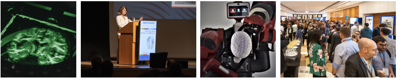
As the ten-year European Flagship Human Brain Project (HBP) approaches its conclusion in September 2023, the final HBP Summit will highlight the scientific achievements of the project at the interface of neuroscience and technology and the legacy that it will leave for the brain research community. …

One last excerpt from the essay,

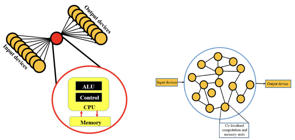
Neuromorphic computing is a radical reimagining of computer architecture at the transistor level, modeled after the structure and function of biological neural networks in the brain. This computing paradigm aims to build electronic systems that attempt to emulate the distributed and parallel computation of the brain by combining processing and memory in the same physical location.

This is unlike traditional computing, which is based on von Neumann systems consisting of three different units: processing unit, I/O unit, and storage unit. This stored program architecture is a model for designing computers that uses a single memory to store both data and instructions, and a central processing unit to execute those instructions. This design, first proposed by mathematician and computer scientist John von Neumann, is widely used in modern computers and is considered to be the standard architecture for computer systems and relies on a clear distinction between memory and processing.

I found the diagram Berger Included with von Neumann’s design contrasted with a neuromorphic design illuminating,

A graphical comparison of the von Neumann and Neuromorphic architecture. Left: The von Neumann architecture used in traditional computers. The red lines depict the data communication bottleneck in the von Neumann architecture. Right: A graphical representation of a general neuromorphic architecture. In this architecture, the processing and memory is decentralized across different neuronal units(the yellow nodes) and synapses(the black lines connecting the nodes), creating a naturally parallel computing environment via the mesh-like structure. (Source: DOI: 10.1109/IS.2016.7737434) [downloaded from https://www.nanowerk.com/spotlight/spotid=62353.php]

Berger offers a very good overview and I recommend reading his February 13, 2023 essay on neuromorphic engineering with one proviso, Note: A link has been removed,

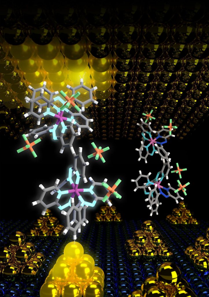
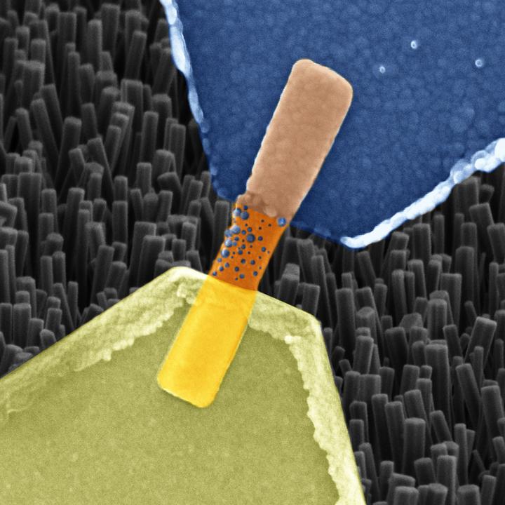
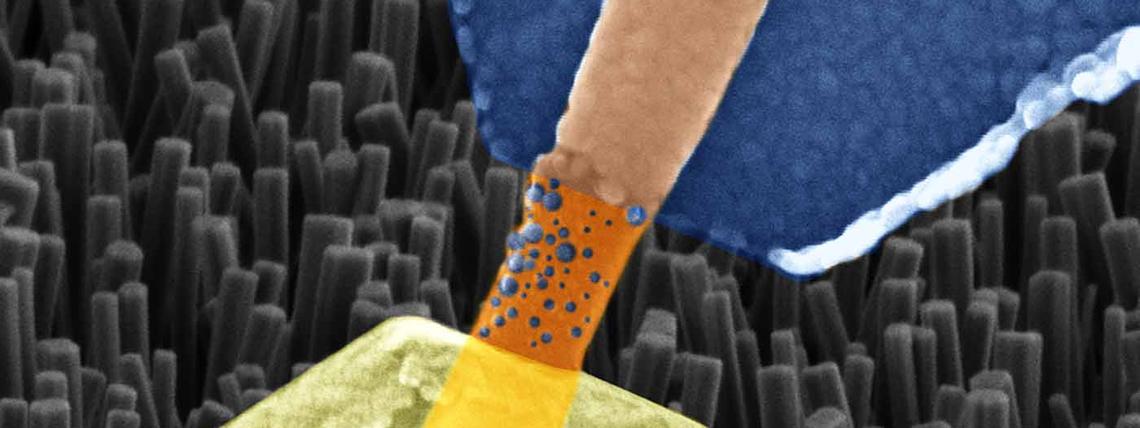
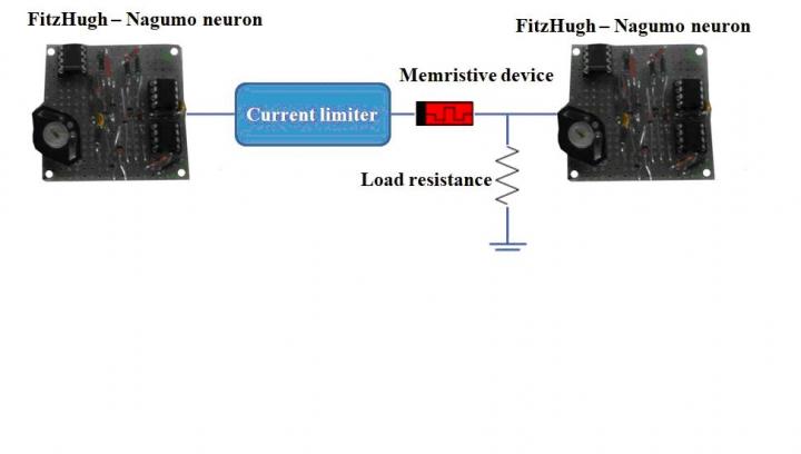
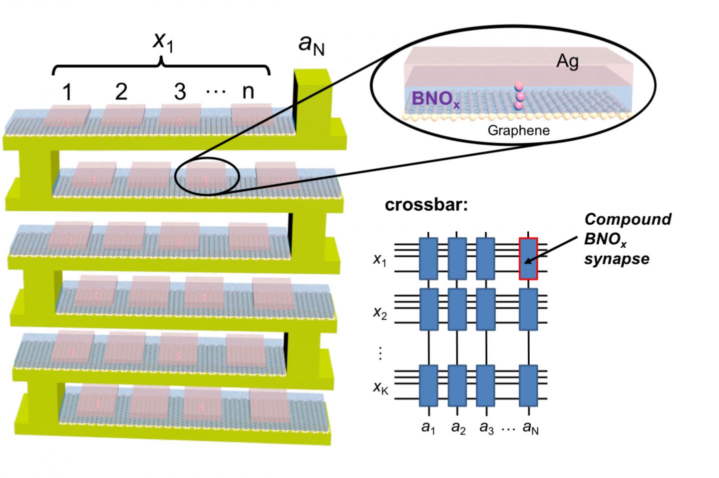
Many researchers in this field see memristors as a key device component for neuromorphic engineering. Memristor – or memory resistor – devices are non-volatile nanoelectronic memory devices that were first theorized [emphasis mine] by Leon Chua in the 1970’s. However, it was some thirty years later that the first practical device was fabricated in 2008 by a group led by Stanley Williams [sometimes cited as R. Stanley Williams] at HP Research Labs.

Chua wasn’t the first as he, himself, has noted. Chua arrived at his theory independently in the 1970s but Bernard Widrow theorized what he called a ‘memistor’ in the 1960s. In fact “Memristors: they are older than you think” is a May 22, 2012 posting which featured an article “Two centuries of memristors” by Themistoklis Prodromakis, Christofer Toumazou and Leon Chua published in Nature Materials.

Most of us try to get it right but we don’t always succeed. It’s always good practice to read everyone (including me) with a little skepticism.

Neurotransistor for brainlike (neuromorphic) computing

According to researchers at Helmholtz-Zentrum Dresden-Rossendorf and the rest of the international team collaborating on the work, it’s time to look more closely at plasticity in the neuronal membrane,.

From the abstract for their paper, Intrinsic plasticity of silicon nanowire neurotransistors for dynamic memory and learning functions by Eunhye Baek, Nikhil Ranjan Das, Carlo Vittorio Cannistraci, Taiuk Rim, Gilbert Santiago Cañón Bermúdez, Khrystyna Nych, Hyeonsu Cho, Kihyun Kim, Chang-Ki Baek, Denys Makarov, Ronald Tetzlaff, Leon Chua, Larysa Baraban & Gianaurelio Cuniberti. Nature Electronics volume 3, pages 398–408 (2020) DOI: https://doi.org/10.1038/s41928-020-0412-1 Published online: 25 May 2020 Issue Date: July 2020

Neuromorphic architectures merge learning and memory functions within a single unit cell and in a neuron-like fashion. Research in the field has been mainly focused on the plasticity of artificial synapses. However, the intrinsic plasticity of the neuronal membrane is also important in the implementation of neuromorphic information processing. Here we report a neurotransistor made from a silicon nanowire transistor coated by an ion-doped sol–gel silicate film that can emulate the intrinsic plasticity of the neuronal membrane.

Caption: Neurotransistors: from silicon chips to neuromorphic architecture. Credit: TU Dresden / E. Baek Courtesy: Helmholtz-Zentrum Dresden-Rossendorf

A July 14, 2020 news item on Nanowerk announced the research (Note: A link has been removed),

Especially activities in the field of artificial intelligence, like teaching robots to walk or precise automatic image recognition, demand ever more powerful, yet at the same time more economical computer chips. While the optimization of conventional microelectronics is slowly reaching its physical limits, nature offers us a blueprint how information can be processed and stored quickly and efficiently: our own brain.

For the very first time, scientists at TU Dresden and the Helmholtz-Zentrum Dresden-Rossendorf (HZDR) have now successfully imitated the functioning of brain neurons using semiconductor materials. They have published their research results in the journal Nature Electronics (“Intrinsic plasticity of silicon nanowire neurotransistors for dynamic memory and learning functions”).

A July 14, 2020 Helmholtz-Zentrum Dresden-Rossendorf press release (also on EurekAlert), which originated the news items delves further into the research,

Today, enhancing the performance of microelectronics is usually achieved by reducing component size, especially of the individual transistors on the silicon computer chips. “But that can’t go on indefinitely – we need new approaches”, Larysa Baraban asserts. The physicist, who has been working at HZDR since the beginning of the year, is one of the three primary authors of the international study, which involved a total of six institutes. One approach is based on the brain, combining data processing with data storage in an artificial neuron.

“Our group has extensive experience with biological and chemical electronic sensors,” Baraban continues. “So, we simulated the properties of neurons using the principles of biosensors and modified a classical field-effect transistor to create an artificial neurotransistor.” The advantage of such an architecture lies in the simultaneous storage and processing of information in a single component. In conventional transistor technology, they are separated, which slows processing time and hence ultimately also limits performance.

Silicon wafer + polymer = chip capable of learning

Modeling computers on the human brain is no new idea. Scientists made attempts to hook up nerve cells to electronics in Petri dishes decades ago. “But a wet computer chip that has to be fed all the time is of no use to anybody,” says Gianaurelio Cuniberti from TU Dresden. The Professor for Materials Science and Nanotechnology is one of the three brains behind the neurotransistor alongside Ronald Tetzlaff, Professor of Fundamentals of Electrical Engineering in Dresden, and Leon Chua [emphasis mine] from the University of California at Berkeley, who had already postulated similar components in the early 1970s.

Now, Cuniberti, Baraban and their team have been able to implement it: “We apply a viscous substance – called solgel – to a conventional silicon wafer with circuits. This polymer hardens and becomes a porous ceramic,” the materials science professor explains. “Ions move between the holes. They are heavier than electrons and slower to return to their position after excitation. This delay, called hysteresis, is what causes the storage effect.” As Cuniberti explains, this is a decisive factor in the functioning of the transistor. “The more an individual transistor is excited, the sooner it will open and let the current flow. This strengthens the connection. The system is learning.”

Cuniberti and his team are not focused on conventional issues, though. “Computers based on our chip would be less precise and tend to estimate mathematical computations rather than calculating them down to the last decimal,” the scientist explains. “But they would be more intelligent. For example, a robot with such processors would learn to walk or grasp; it would possess an optical system and learn to recognize connections. And all this without having to develop any software.” But these are not the only advantages of neuromorphic computers. Thanks to their plasticity, which is similar to that of the human brain, they can adapt to changing tasks during operation and, thus, solve problems for which they were not originally programmed.

I highlighted Dr. Leon Chua’s name as he was one of the first to conceptualize the notion of a memristor (memory resistor), which is what the press release seems to be referencing with the mention of artificial synapses. Dr. Chua very kindly answered a few questions for me about his work which I published in an April 13, 2010 posting (scroll down about 40% of the way).

Brain-inspired electronics with organic memristors for wearable computing

I went down a rabbit hole while trying to figure out the difference between ‘organic’ memristors and standard memristors. I have put the results of my investigation at the end of this post. First, there’s the news.

An April 21, 2020 news item on ScienceDaily explains why researchers are so focused on memristors and brainlike computing,

The advent of artificial intelligence, machine learning and the internet of things is expected to change modern electronics and bring forth the fourth Industrial Revolution. The pressing question for many researchers is how to handle this technological revolution.

“It is important for us to understand that the computing platforms of today will not be able to sustain at-scale implementations of AI algorithms on massive datasets,” said Thirumalai Venkatesan, one of the authors of a paper published in Applied Physics Reviews, from AIP Publishing.

“Today’s computing is way too energy-intensive to handle big data. We need to rethink our approaches to computation on all levels: materials, devices and architecture that can enable ultralow energy computing.”

An April 21, 2020 American Institute of Physics (AIP) news release (also on EurekAlert), which originated the news item, describes the authors’ approach to the problems with organic memristors,

Brain-inspired electronics with organic memristors could offer a functionally promising and cost- effective platform, according to Venkatesan. Memristive devices are electronic devices with an inherent memory that are capable of both storing data and performing computation. Since memristors are functionally analogous to the operation of neurons, the computing units in the brain, they are optimal candidates for brain-inspired computing platforms.

Until now, oxides have been the leading candidate as the optimum material for memristors. Different material systems have been proposed but none have been successful so far.

“Over the last 20 years, there have been several attempts to come up with organic memristors, but none of those have shown any promise,” said Sreetosh Goswami, lead author on the paper. “The primary reason behind this failure is their lack of stability, reproducibility and ambiguity in mechanistic understanding. At a device level, we are now able to solve most of these problems,”

This new generation of organic memristors is developed based on metal azo complex devices, which are the brainchild of Sreebata Goswami, a professor at the Indian Association for the Cultivation of Science in Kolkata and another author on the paper.

“In thin films, the molecules are so robust and stable that these devices can eventually be the right choice for many wearable and implantable technologies or a body net, because these could be bendable and stretchable,” said Sreebata Goswami. A body net is a series of wireless sensors that stick to the skin and track health.

The next challenge will be to produce these organic memristors at scale, said Venkatesan.

“Now we are making individual devices in the laboratory. We need to make circuits for large-scale functional implementation of these devices.”

Caption: The device structure at a molecular level. The gold nanoparticles on the bottom electrode enhance the field enabling an ultra-low energy operation of the molecular device. Credit Sreetosh Goswami, Sreebrata Goswami and Thirumalai Venky Venkatesan

Here’s a link to and a citation for the paper,

An organic approach to low energy memory and brain inspired electronics by Sreetosh Goswami, Sreebrata Goswami, and T. Venkatesan. Applied Physics Reviews 7, 021303 (2020) DOI: https://doi.org/10.1063/1.5124155

This paper is open access.

Basics about memristors and organic memristors

This undated article on Nanowerk provides a relatively complete and technical description of memristors in general (Note: A link has been removed),

A memristor (named as a portmanteau of memory and resistor) is a non-volatile electronic memory device that was first theorized by Leon Ong Chua in 1971 as the fourth fundamental two-terminal circuit element following the resistor, the capacitor, and the inductor (IEEE Transactions on Circuit Theory, “Memristor-The missing circuit element”).

Its special property is that its resistance can be programmed (resistor function) and subsequently remains stored (memory function). Unlike other memories that exist today in modern electronics, memristors are stable and remember their state even if the device loses power.

However, it was only almost 40 years later that the first practical device was fabricated. This was in 2008, when a group led by Stanley Williams at HP Research Labs realized that switching of the resistance between a conducting and less conducting state in metal-oxide thin-film devices was showing Leon Chua’s memristor behavior. …

The article on Nanowerk includes an embedded video presentation on memristors given by Stanley Williams (also known as R. Stanley Williams).

Mention of an ‘organic’memristor can be found in an October 31, 2017 article by Ryan Whitwam,

The memristor is composed of the transition metal ruthenium complexed with “azo-aromatic ligands.” [emphasis mine] The theoretical work enabling this material was performed at Yale, and the organic molecules were synthesized at the Indian Association for the Cultivation of Sciences. …

I highlighted ‘ligands’ because that appears to be the difference. However, there is more than one type of ligand on Wikipedia.

First, there’s the Ligand (biochemistry) entry (Note: Links have been removed),

In biochemistry and pharmacology, a ligand is a substance that forms a complex with a biomolecule to serve a biological purpose. …

Then, there’s the Ligand entry,

In coordination chemistry, a ligand[help 1] is an ion or molecule (functional group) that binds to a central metal atom to form a coordination complex …

Finally, there’s the Ligand (disambiguation) entry (Note: Links have been removed),

  • Ligand, an atom, ion, or functional group that donates one or more of its electrons through a coordinate covalent bond to one or more central atoms or ions
  • Ligand (biochemistry), a substance that binds to a protein
  • a ‘guest’ in host–guest chemistry

I did take a look at the paper and did not see any references to proteins or other biomolecules that I could recognize as such. I’m not sure why the researchers are describing their device as an ‘organic’ memristor but this may reflect a shortcoming in the definitions I have found or shortcomings in my reading of the paper rather than an error on their parts.

Hopefully, more research will be forthcoming and it will be possible to better understand the terminology.

An artificial synapse tuned by light, a ferromagnetic memristor, and a transparent, flexible artificial synapse

Down the memristor rabbit hole one more time.* I started out with news about two new papers and inadvertently found two more. In a bid to keep this posting to a manageable size, I’m stopping at four.

UK

In a June 19, 2019 Nanowerk Spotlight article, Dr. Neil Kemp discusses memristors and some of his latest work (Note: A link has been removed),

Memristor (or memory resistors) devices are non-volatile electronic memory devices that were first theorized by Leon Chua in the 1970’s. However, it was some thirty years later that the first practical device was fabricated. This was in 2008 when a group led by Stanley Williams at HP Research Labs realized that switching of the resistance between a conducting and less conducting state in metal-oxide thin-film devices was showing Leon Chua’s memristor behaviour.

The high interest in memristor devices also stems from the fact that these devices emulate the memory and learning properties of biological synapses. i.e. the electrical resistance value of the device is dependent on the history of the current flowing through it.

There is a huge effort underway to use memristor devices in neuromorphic computing applications and it is now reasonable to imagine the development of a new generation of artificial intelligent devices with very low power consumption (non-volatile), ultra-fast performance and high-density integration.

These discoveries come at an important juncture in microelectronics, since there is increasing disparity between computational needs of Big Data, Artificial Intelligence (A.I.) and the Internet of Things (IoT), and the capabilities of existing computers. The increases in speed, efficiency and performance of computer technology cannot continue in the same manner as it has done since the 1960s.

To date, most memristor research has focussed on the electronic switching properties of the device. However, for many applications it is useful to have an additional handle (or degree of freedom) on the device to control its resistive state. For example memory and processing in the brain also involves numerous chemical and bio-chemical reactions that control the brain structure and its evolution through development.

To emulate this in a simple solid-state system composed of just switches alone is not possible. In our research, we are interested in using light to mediate this essential control.

We have demonstrated that light can be used to make short and long-term memory and we have shown how light can modulate a special type of learning, called spike timing dependent plasticity (STDP). STDP involves two neuronal spikes incident across a synapse at the same time. Depending on the relative timing of the spikes and their overlap across the synaptic cleft, the connection strength is other strengthened or weakened.

In our earlier work, we were only able to achieve to small switching effects in memristors using light. In our latest work (Advanced Electronic Materials, “Percolation Threshold Enables Optical Resistive-Memory Switching and Light-Tuneable Synaptic Learning in Segregated Nanocomposites”), we take advantage of a percolating-like nanoparticle morphology to vastly increase the magnitude of the switching between electronic resistance states when light is incident on the device.

We have used an inhomogeneous percolating network consisting of metallic nanoparticles distributed in filamentary-like conduction paths. Electronic conduction and the resistance of the device is very sensitive to any disruption of the conduction path(s).

By embedding the nanoparticles in a polymer that can expand or contract with light the conduction pathways are broken or re-connected causing very large changes in the electrical resistance and memristance of the device.

Our devices could lead to the development of new memristor-based artificial intelligence systems that are adaptive and reconfigurable using a combination of optical and electronic signalling. Furthermore, they have the potential for the development of very fast optical cameras for artificial intelligence recognition systems.

Our work provides a nice proof-of-concept but the materials used means the optical switching is slow. The materials are also not well suited to industry fabrication. In our on-going work we are addressing these switching speed issues whilst also focussing on industry compatible materials.

Currently we are working on a new type of optical memristor device that should give us orders of magnitude improvement in the optical switching speeds whilst also retaining a large difference between the resistance on and off states. We hope to be able to achieve nanosecond switching speeds. The materials used are also compatible with industry standard methods of fabrication.

The new devices should also have applications in optical communications, interfacing and photonic computing. We are currently looking for commercial investors to help fund the research on these devices so that we can bring the device specifications to a level of commercial interest.

If you’re interested in memristors, Kemp’s article is well written and quite informative for nonexperts, assuming of course you can tolerate not understanding everything perfectly.

Here are links and citations for two papers. The first is the latest referred to in the article, a May 2019 paper and the second is a paper appearing in July 2019.

Percolation Threshold Enables Optical Resistive‐Memory Switching and Light‐Tuneable Synaptic Learning in Segregated Nanocomposites by Ayoub H. Jaafar, Mary O’Neill, Stephen M. Kelly, Emanuele Verrelli, Neil T. Kemp. Advanced Electronic Materials DOI: https://doi.org/10.1002/aelm.201900197 First published: 28 May 2019

Wavelength dependent light tunable resistive switching graphene oxide nonvolatile memory devices by Ayoub H.Jaafar, N.T.Kemp. DOI: https://doi.org/10.1016/j.carbon.2019.07.007 Carbon Available online 3 July 2019

The first paper (May 2019) is definitely behind a paywall and the second paper (July 2019) appears to be behind a paywall.

Dr. Kemp’s work has been featured here previously in a January 3, 2018 posting in the subsection titled, Shining a light on the memristor.

China

This work from China was announced in a June 20, 2019 news item on Nanowerk,

Memristors, demonstrated by solid-state devices with continuously tunable resistance, have emerged as a new paradigm for self-adaptive networks that require synapse-like functions. Spin-based memristors offer advantages over other types of memristors because of their significant endurance and high energy effciency.

However, it remains a challenge to build dense and functional spintronic memristors with structures and materials that are compatible with existing ferromagnetic devices. Ta/CoFeB/MgO heterostructures are commonly used in interfacial PMA-based [perpendicular magnetic anisotropy] magnetic tunnel junctions, which exhibit large tunnel magnetoresistance and are implemented in commercial MRAM [magnetic random access memory] products.

“To achieve the memristive function, DW is driven back and forth in a continuous manner in the CoFeB layer by applying in-plane positive or negative current pulses along the Ta layer, utilizing SOT that the current exerts on the CoFeB magnetization,” said Shuai Zhang, a coauthor in the paper. “Slowly propagating domain wall generates a creep in the detection area of the device, which yields a broad range of intermediate resistive states in the AHE [anomalous Hall effect] measurements. Consequently, AHE resistance is modulated in an analog manner, being controlled by the pulsed current characteristics including amplitude, duration, and repetition number.”

“For a follow-up study, we are working on more neuromorphic operations, such as spike-timing-dependent plasticity and paired pulsed facilitation,” concludes You. …

Here’s are links to and citations for the paper (Note: It’s a little confusing but I believe that one of the links will take you to the online version, as for the ‘open access’ link, keep reading),

A Spin–Orbit‐Torque Memristive Device by Shuai Zhang, Shijiang Luo, Nuo Xu, Qiming Zou, Min Song, Jijun Yun, Qiang Luo, Zhe Guo, Ruofan Li, Weicheng Tian, Xin Li, Hengan Zhou, Huiming Chen, Yue Zhang, Xiaofei Yang, Wanjun Jiang, Ka Shen, Jeongmin Hong, Zhe Yuan, Li Xi, Ke Xia, Sayeef Salahuddin, Bernard Dieny, Long You. Advanced Electronic Materials Volume 5, Issue 4 April 2019 (print version) 1800782 DOI: https://doi.org/10.1002/aelm.201800782 First published [online]: 30 January 2019 Note: there is another DOI, https://doi.org/10.1002/aelm.201970022 where you can have open access to Memristors: A Spin–Orbit‐Torque Memristive Device (Adv. Electron. Mater. 4/2019)

The paper published online in January 2019 is behind a paywall and the paper (almost the same title) published in April 2019 has a new DOI and is open access. Final note: I tried accessing the ‘free’ paper and opened up a free file for the artwork featuring the work from China on the back cover of the April 2019 of Advanced Electronic Materials.

Korea

Usually when I see the words transparency and flexibility, I expect to see graphene is one of the materials. That’s not the case for this paper (link to and citation for),

Transparent and flexible photonic artificial synapse with piezo-phototronic modulator: Versatile memory capability and higher order learning algorithm by Mohit Kumar, Joondong Kim, Ching-Ping Wong. Nano Energy Volume 63, September 2019, 103843 DOI: https://doi.org/10.1016/j.nanoen.2019.06.039 Available online 22 June 2019

Here’s the abstract for the paper where you’ll see that the material is made up of zinc oxide silver nanowires,

An artificial photonic synapse having tunable manifold synaptic response can be an essential step forward for the advancement of novel neuromorphic computing. In this work, we reported the development of highly transparent and flexible two-terminal ZnO/Ag-nanowires/PET photonic artificial synapse [emphasis mine]. The device shows purely photo-triggered all essential synaptic functions such as transition from short-to long-term plasticity, paired-pulse facilitation, and spike-timing-dependent plasticity, including in the versatile memory capability. Importantly, strain-induced piezo-phototronic effect within ZnO provides an additional degree of regulation to modulate all of the synaptic functions in multi-levels. The observed effect is quantitatively explained as a dynamic of photo-induced electron-hole trapping/detraining via the defect states such as oxygen vacancies. We revealed that the synaptic functions can be consolidated and converted by applied strain, which is not previously applied any of the reported synaptic devices. This study will open a new avenue to the scientific community to control and design highly transparent wearable neuromorphic computing.

This paper is behind a paywall.

Artificial synapse courtesy of nanowires

It looks like a popsicle to me,

Caption: Image captured by an electron microscope of a single nanowire memristor (highlighted in colour to distinguish it from other nanowires in the background image). Blue: silver electrode, orange: nanowire, yellow: platinum electrode. Blue bubbles are dispersed over the nanowire. They are made up of silver ions and form a bridge between the electrodes which increases the resistance. Credit: Forschungszentrum Jülich

Not a popsicle but a representation of a device (memristor) scientists claim mimics a biological nerve cell according to a December 5, 2018 news item on ScienceDaily,

Scientists from Jülich [Germany] together with colleagues from Aachen [Germany] and Turin [Italy] have produced a memristive element made from nanowires that functions in much the same way as a biological nerve cell. The component is able to both save and process information, as well as receive numerous signals in parallel. The resistive switching cell made from oxide crystal nanowires is thus proving to be the ideal candidate for use in building bioinspired “neuromorphic” processors, able to take over the diverse functions of biological synapses and neurons.

A Dec. 5, 2018 Forschungszentrum Jülich press release (also on EurekAlert), which originated the news item, provides more details,

Computers have learned a lot in recent years. Thanks to rapid progress in artificial intelligence they are now able to drive cars, translate texts, defeat world champions at chess, and much more besides. In doing so, one of the greatest challenges lies in the attempt to artificially reproduce the signal processing in the human brain. In neural networks, data are stored and processed to a high degree in parallel. Traditional computers on the other hand rapidly work through tasks in succession and clearly distinguish between the storing and processing of information. As a rule, neural networks can only be simulated in a very cumbersome and inefficient way using conventional hardware.

Systems with neuromorphic chips that imitate the way the human brain works offer significant advantages. Experts in the field describe this type of bioinspired computer as being able to work in a decentralised way, having at its disposal a multitude of processors, which, like neurons in the brain, are connected to each other by networks. If a processor breaks down, another can take over its function. What is more, just like in the brain, where practice leads to improved signal transfer, a bioinspired processor should have the capacity to learn.

“With today’s semiconductor technology, these functions are to some extent already achievable. These systems are however suitable for particular applications and require a lot of space and energy,” says Dr. Ilia Valov from Forschungszentrum Jülich. “Our nanowire devices made from zinc oxide crystals can inherently process and even store information, as well as being extremely small and energy efficient,” explains the researcher from Jülich’s Peter Grünberg Institute.

For years memristive cells have been ascribed the best chances of being capable of taking over the function of neurons and synapses in bioinspired computers. They alter their electrical resistance depending on the intensity and direction of the electric current flowing through them. In contrast to conventional transistors, their last resistance value remains intact even when the electric current is switched off. Memristors are thus fundamentally capable of learning.

In order to create these properties, scientists at Forschungszentrum Jülich and RWTH Aachen University used a single zinc oxide nanowire, produced by their colleagues from the polytechnic university in Turin. Measuring approximately one ten-thousandth of a millimeter in size, this type of nanowire is over a thousand times thinner than a human hair. The resulting memristive component not only takes up a tiny amount of space, but also is able to switch much faster than flash memory.

Nanowires offer promising novel physical properties compared to other solids and are used among other things in the development of new types of solar cells, sensors, batteries and computer chips. Their manufacture is comparatively simple. Nanowires result from the evaporation deposition of specified materials onto a suitable substrate, where they practically grow of their own accord.

In order to create a functioning cell, both ends of the nanowire must be attached to suitable metals, in this case platinum and silver. The metals function as electrodes, and in addition, release ions triggered by an appropriate electric current. The metal ions are able to spread over the surface of the wire and build a bridge to alter its conductivity.

Components made from single nanowires are, however, still too isolated to be of practical use in chips. Consequently, the next step being planned by the Jülich and Turin researchers is to produce and study a memristive element, composed of a larger, relatively easy to generate group of several hundred nanowires offering more exciting functionalities.

The Italians have also written about the work in a December 4, 2018 news item for the Polytecnico di Torino’s inhouse magazine, PoliFlash’. I like the image they’ve used better as it offers a bit more detail and looks less like a popsicle. First, the image,

Courtesy: Polytecnico di Torino

Now, the news item, which includes some historical information about the memristor (Note: There is some repetition and links have been removed),

Emulating and understanding the human brain is one of the most important challenges for modern technology: on the one hand, the ability to artificially reproduce the processing of brain signals is one of the cornerstones for the development of artificial intelligence, while on the other the understanding of the cognitive processes at the base of the human mind is still far away.

And the research published in the prestigious journal Nature Communications by Gianluca Milano and Carlo Ricciardi, PhD student and professor, respectively, of the Applied Science and Technology Department of the Politecnico di Torino, represents a step forward in these directions. In fact, the study entitled “Self-limited single nanowire systems combining all-in-one memristive and neuromorphic functionalities” shows how it is possible to artificially emulate the activity of synapses, i.e. the connections between neurons that regulate the learning processes in our brain, in a single “nanowire” with a diameter thousands of times smaller than that of a hair.

It is a crystalline nanowire that takes the “memristor”, the electronic device able to artificially reproduce the functions of biological synapses, to a more performing level. Thanks to the use of nanotechnologies, which allow the manipulation of matter at the atomic level, it was for the first time possible to combine into one single device the synaptic functions that were individually emulated through specific devices. For this reason, the nanowire allows an extreme miniaturisation of the “memristor”, significantly reducing the complexity and energy consumption of the electronic circuits necessary for the implementation of learning algorithms.

Starting from the theorisation of the “memristor” in 1971 by Prof. Leon Chua – now visiting professor at the Politecnico di Torino, who was conferred an honorary degree by the University in 2015 – this new technology will not only allow smaller and more performing devices to be created for the implementation of increasingly “intelligent” computers, but is also a significant step forward for the emulation and understanding of the functioning of the brain.

“The nanowire memristor – said Carlo Ricciardirepresents a model system for the study of physical and electrochemical phenomena that govern biological synapses at the nanoscale. The work is the result of the collaboration between our research team and the RWTH University of Aachen in Germany, supported by INRiM, the National Institute of Metrological Research, and IIT, the Italian Institute of Technology.”

h.t for the Italian info. to Nanowerk’s Dec. 10, 2018 news item.

Here’s a link to and a citation for the paper,

Self-limited single nanowire systems combining all-in-one memristive and neuromorphic functionalities by Gianluca Milano, Michael Luebben, Zheng Ma, Rafal Dunin-Borkowski, Luca Boarino, Candido F. Pirri, Rainer Waser, Carlo Ricciardi, & Ilia Valov. Nature Communicationsvolume 9, Article number: 5151 (2018) DOI: https://doi.org/10.1038/s41467-018-07330-7 Published: 04 December 2018

This paper is open access.

Just use the search term “memristor” in the blog search engine if you’re curious about the multitudinous number of postings on the topic here.

Two approaches to memristors

Within one day of each other in October 2018, two different teams working on memristors with applications to neuroprosthetics and neuromorphic computing (brainlike computing) announced their results.

Russian team

An October 15, 2018 (?) Lobachevsky University press release (also published on October 15, 2018 on EurekAlert) describes a new approach to memristors,

Biological neurons are coupled unidirectionally through a special junction called a synapse. An electrical signal is transmitted along a neuron after some biochemical reactions initiate a chemical release to activate an adjacent neuron. These junctions are crucial for cognitive functions, such as perception, learning and memory.

A group of researchers from Lobachevsky University in Nizhny Novgorod investigates the dynamics of an individual memristive device when it receives a neuron-like signal as well as the dynamics of a network of analog electronic neurons connected by means of a memristive device. According to Svetlana Gerasimova, junior researcher at the Physics and Technology Research Institute and at the Neurotechnology Department of Lobachevsky University, this system simulates the interaction between synaptically coupled brain neurons while the memristive device imitates a neuron axon.

A memristive device is a physical model of Chua’s [Dr. Leon Chua, University of California at Berkeley; see my May 9, 2008 posting for a brief description Dr. Chua’s theory] memristor, which is an electric circuit element capable of changing its resistance depending on the electric signal received at the input. The device based on a Au/ZrO2(Y)/TiN/Ti structure demonstrates reproducible bipolar switching between the low and high resistance states. Resistive switching is determined by the oxidation and reduction of segments of conducting channels (filaments) in the oxide film when voltage with different polarity is applied to it. In the context of the present work, the ability of a memristive device to change conductivity under the action of pulsed signals makes it an almost ideal electronic analog of a synapse.

Lobachevsky University scientists and engineers supported by the Russian Science Foundation (project No.16-19-00144) have experimentally implemented and theoretically described the synaptic connection of neuron-like generators using the memristive interface and investigated the characteristics of this connection.

“Each neuron is implemented in the form of a pulse signal generator based on the FitzHugh-Nagumo model. This model provides a qualitative description of the main neurons’ characteristics: the presence of the excitation threshold, the presence of excitable and self-oscillatory regimes with the possibility of a changeover. At the initial time moment, the master generator is in the self-oscillatory mode, the slave generator is in the excitable mode, and the memristive device is used as a synapse. The signal from the master generator is conveyed to the input of the memristive device, the signal from the output of the memristive device is transmitted to the input of the slave generator via the loading resistance. When the memristive device switches from a high resistance to a low resistance state, the connection between the two neuron-like generators is established. The master generator goes into the oscillatory mode and the signals of the generators are synchronized. Different signal modulation mode synchronizations were demonstrated for the Au/ZrO2(Y)/TiN/Ti memristive device,” – says Svetlana Gerasimova.

UNN researchers believe that the next important stage in the development of neuromorphic systems based on memristive devices is to apply such systems in neuroprosthetics. Memristive systems will provide a highly efficient imitation of synaptic connection due to the stochastic nature of the memristive phenomenon and can be used to increase the flexibility of the connections for neuroprosthetic purposes. Lobachevsky University scientists have vast experience in the development of neurohybrid systems. In particular, a series of experiments was performed with the aim of connecting the FitzHugh-Nagumo oscillator with a biological object, a rat brain hippocampal slice. The signal from the electronic neuron generator was transmitted through the optic fiber communication channel to the bipolar electrode which stimulated Schaffer collaterals (axons of pyramidal neurons in the CA3 field) in the hippocampal slices. “We are going to combine our efforts in the design of artificial neuromorphic systems and our experience of working with living cells to improve flexibility of prosthetics,” concludes S. Gerasimova.

The results of this research were presented at the 38th International Conference on Nonlinear Dynamics (Dynamics Days Europe) at Loughborough University (Great Britain).

This diagram illustrates an aspect of the work,

Caption: Schematic of electronic neurons coupling via a memristive device. Credit: Lobachevsky University

US team

The American Institute of Physics (AIP) announced the publication of a ‘memristor paper’ by a team from the University of Southern California (USC) in an October 16, 2018 news item on phys.org,

Just like their biological counterparts, hardware that mimics the neural circuitry of the brain requires building blocks that can adjust how they synapse, with some connections strengthening at the expense of others. One such approach, called memristors, uses current resistance to store this information. New work looks to overcome reliability issues in these devices by scaling memristors to the atomic level.

An October 16, 2018 AIP news release (also on EurekAlert), which originated the news item, delves further into the particulars of this particular piece of memristor research,

A group of researchers demonstrated a new type of compound synapse that can achieve synaptic weight programming and conduct vector-matrix multiplication with significant advances over the current state of the art. Publishing its work in the Journal of Applied Physics, from AIP Publishing, the group’s compound synapse is constructed with atomically thin boron nitride memristors running in parallel to ensure efficiency and accuracy.

The article appears in a special topic section of the journal devoted to “New Physics and Materials for Neuromorphic Computation,” which highlights new developments in physical and materials science research that hold promise for developing the very large-scale, integrated “neuromorphic” systems of tomorrow that will carry computation beyond the limitations of current semiconductors today.

“There’s a lot of interest in using new types of materials for memristors,” said Ivan Sanchez Esqueda, an author on the paper. “What we’re showing is that filamentary devices can work well for neuromorphic computing applications, when constructed in new clever ways.”

Current memristor technology suffers from a wide variation in how signals are stored and read across devices, both for different types of memristors as well as different runs of the same memristor. To overcome this, the researchers ran several memristors in parallel. The combined output can achieve accuracies up to five times those of conventional devices, an advantage that compounds as devices become more complex.

The choice to go to the subnanometer level, Sanchez said, was born out of an interest to keep all of these parallel memristors energy-efficient. An array of the group’s memristors were found to be 10,000 times more energy-efficient than memristors currently available.

“It turns out if you start to increase the number of devices in parallel, you can see large benefits in accuracy while still conserving power,” Sanchez said. Sanchez said the team next looks to further showcase the potential of the compound synapses by demonstrating their use completing increasingly complex tasks, such as image and pattern recognition.

Here’s an image illustrating the parallel artificial synapses,

Caption: Hardware that mimics the neural circuitry of the brain requires building blocks that can adjust how they synapse. One such approach, called memristors, uses current resistance to store this information. New work looks to overcome reliability issues in these devices by scaling memristors to the atomic level. Researchers demonstrated a new type of compound synapse that can achieve synaptic weight programming and conduct vector-matrix multiplication with significant advances over the current state of the art. They discuss their work in this week’s Journal of Applied Physics. This image shows a conceptual schematic of the 3D implementation of compound synapses constructed with boron nitride oxide (BNOx) binary memristors, and the crossbar array with compound BNOx synapses for neuromorphic computing applications. Credit: Ivan Sanchez Esqueda

Here’s a link to and a citation for the paper,

Efficient learning and crossbar operations with atomically-thin 2-D material compound synapses by Ivan Sanchez Esqueda, Huan Zhao and Han Wang. The article will appear in the Journal of Applied Physics Oct. 16, 2018 (DOI: 10.1063/1.5042468).

This paper is behind a paywall.

*Title corrected from ‘Two approaches to memristors featuring’ to ‘Two approaches to memristors’ on May 31, 2019 at 1455 hours PDT.

Mott memristor

Mott memristors (mentioned in my Aug. 24, 2017 posting about neuristors and brainlike computing) gets more fulsome treatment in an Oct. 9, 2017 posting by Samuel K. Moore on the Nanoclast blog (found on the IEEE [Institute of Electrical and Electronics Engineers] website) Note: 1: Links have been removed; Note 2 : I quite like Moore’s writing style but he’s not for the impatient reader,

When you’re really harried, you probably feel like your head is brimful of chaos. You’re pretty close. Neuroscientists say your brain operates in a regime termed the “edge of chaos,” and it’s actually a good thing. It’s a state that allows for fast, efficient analog computation of the kind that can solve problems that grow vastly more difficult as they become bigger in size.

The trouble is, if you’re trying to replicate that kind of chaotic computation with electronics, you need an element that both acts chaotically—how and when you want it to—and could scale up to form a big system.

“No one had been able to show chaotic dynamics in a single scalable electronic device,” says Suhas Kumar, a researcher at Hewlett Packard Labs, in Palo Alto, Calif. Until now, that is.

He, John Paul Strachan, and R. Stanley Williams recently reported in the journal Nature that a particular configuration of a certain type of memristor contains that seed of controlled chaos. What’s more, when they simulated wiring these up into a type of circuit called a Hopfield neural network, the circuit was capable of solving a ridiculously difficult problem—1,000 instances of the traveling salesman problem—at a rate of 10 trillion operations per second per watt.

(It’s not an apples-to-apples comparison, but the world’s most powerful supercomputer as of June 2017 managed 93,015 trillion floating point operations per second but consumed 15 megawatts doing it. So about 6 billion operations per second per watt.)

The device in question is called a Mott memristor. Memristors generally are devices that hold a memory, in the form of resistance, of the current that has flowed through them. The most familiar type is called resistive RAM (or ReRAM or RRAM, depending on who’s asking). Mott memristors have an added ability in that they can also reflect a temperature-driven change in resistance.

The HP Labs team made their memristor from an 8-nanometer-thick layer of niobium dioxide (NbO2) sandwiched between two layers of titanium nitride. The bottom titanium nitride layer was in the form of a 70-nanometer wide pillar. “We showed that this type of memristor can generate chaotic and nonchaotic signals,” says Williams, who invented the memristor based on theory by Leon Chua.

(The traveling salesman problem is one of these. In it, the salesman must find the shortest route that lets him visit all of his customers’ cities, without going through any of them twice. It’s a difficult problem because it becomes exponentially more difficult to solve with each city you add.)

Here’s what the niobium dioxide-based Mott memristor looks like,

Photo: Suhas Kumar/Hewlett Packard Labs
A micrograph shows the construction of a Mott memristor composed of an 8-nanometer-thick layer of niobium dioxide between two layers of titanium nitride.

Here’s a link to and a citation for the paper,

Chaotic dynamics in nanoscale NbO2 Mott memristors for analogue computing by Suhas Kumar, John Paul Strachan & R. Stanley Williams. Nature 548, 318–321 (17 August 2017) doi:10.1038/nature23307 Published online: 09 August 2017

This paper is behind a paywall.

The memristor as the ‘missing link’ in bioelectronic medicine?

The last time I featured memrisors and a neuronal network it was in an April 22, 2016 posting about Russian research in that field. This latest work comes from the UK’s University of Southampton. From a Sept. 27, 2016 news item on phys.org,

New research, led by the University of Southampton, has demonstrated that a nanoscale device, called a memristor, could be the ‘missing link’ in the development of implants that use electrical signals from the brain to help treat medical conditions.

Monitoring neuronal cell activity is fundamental to neuroscience and the development of neuroprosthetics – biomedically engineered devices that are driven by neural activity. However, a persistent problem is the device being able to process the neural data in real-time, which imposes restrictive requirements on bandwidth, energy and computation capacity.

In a new study, published in Nature Communications, the researchers showed that memristors could provide real-time processing of neuronal signals (spiking events) leading to efficient data compression and the potential to develop more precise and affordable neuroprosthetics and bioelectronic medicines.

A Sept. 27, 2016 University of Southampton press release, which originated the news item, expands on the theme,

Memristors are electrical components that limit or regulate the flow of electrical current in a circuit and can remember the amount of charge that was flowing through it and retain the data, even when the power is turned off.

Lead author Isha Gupta, Postgraduate Research Student at the University of Southampton, said: “Our work can significantly contribute towards further enhancing the understanding of neuroscience, developing neuroprosthetics and bio-electronic medicines by building tools essential for interpreting the big data in a more effective way.”

The research team developed a nanoscale Memristive Integrating Sensor (MIS) into which they fed a series of voltage-time samples, which replicated neuronal electrical activity.

Acting like synapses in the brain, the metal-oxide MIS was able to encode and compress (up to 200 times) neuronal spiking activity recorded by multi-electrode arrays. Besides addressing the bandwidth constraints, this approach was also very power efficient – the power needed per recording channel was up to 100 times less when compared to current best practice.

Co-author Dr Themis Prodromakis, Reader in Nanoelectronics and EPSRC Fellow in Electronics and Computer Science at the University of Southampton said: “We are thrilled that we succeeded in demonstrating that these emerging nanoscale devices, despite being rather simple in architecture, possess ultra-rich dynamics that can be harnessed beyond the obvious memory applications to address the fundamental constraints in bandwidth and power that currently prohibit scaling neural interfaces beyond 1,000 recording channels.”

The Prodromakis Group at the University of Southampton is acknowledged as world-leading in this field, collaborating among others with Leon Chua (a Diamond Jubilee Visiting Academic at the University of Southampton), who theoretically predicted the existence of memristors in 1971.

Here’s a link to and a citation for the paper,

Real-time encoding and compression of neuronal spikes by metal-oxide memristors by Isha Gupta, Alexantrou Serb, Ali Khiat, Ralf Zeitler, Stefano Vassanelli, & Themistoklis Prodromakis. Nature Communications 7, Article number: 12805 doi:10.1038/ncomms12805 Published  26 September 2016

This is an open access paper.

For anyone who’s interested in better understanding memristors, there’s an interview with Forrest H Bennett III in my April 7, 2010 posting and you can always check Wikipedia.

X-rays reveal memristor workings

A June 14, 2016 news item on ScienceDaily focuses on memristors. (It’s been about two months since my last memristor posting on April 22, 2016 regarding electronic synapses and neural networks). This piece announces new insight into how memristors function at the atomic scale,

In experiments at two Department of Energy national labs — SLAC National Accelerator Laboratory and Lawrence Berkeley National Laboratory — scientists at Hewlett Packard Enterprise (HPE) [also referred to as HP Labs or Hewlett Packard Laboratories] have experimentally confirmed critical aspects of how a new type of microelectronic device, the memristor, works at an atomic scale.

This result is an important step in designing these solid-state devices for use in future computer memories that operate much faster, last longer and use less energy than today’s flash memory. …

“We need information like this to be able to design memristors that will succeed commercially,” said Suhas Kumar, an HPE scientist and first author on the group’s technical paper.

A June 13, 2016 SLAC news release, which originated the news item, offers a brief history according to HPE and provides details about the latest work,

The memristor was proposed theoretically [by Dr. Leon Chua] in 1971 as the fourth basic electrical device element alongside the resistor, capacitor and inductor. At its heart is a tiny piece of a transition metal oxide sandwiched between two electrodes. Applying a positive or negative voltage pulse dramatically increases or decreases the memristor’s electrical resistance. This behavior makes it suitable for use as a “non-volatile” computer memory that, like flash memory, can retain its state without being refreshed with additional power.

Over the past decade, an HPE group led by senior fellow R. Stanley Williams has explored memristor designs, materials and behavior in detail. Since 2009 they have used intense synchrotron X-rays to reveal the movements of atoms in memristors during switching. Despite advances in understanding the nature of this switching, critical details that would be important in designing commercially successful circuits  remained controversial. For example, the forces that move the atoms, resulting in dramatic resistance changes during switching, remain under debate.

In recent years, the group examined memristors made with oxides of titanium, tantalum and vanadium. Initial experiments revealed that switching in the tantalum oxide devices could be controlled most easily, so it was chosen for further exploration at two DOE Office of Science User Facilities – SLAC’s Stanford Synchrotron Radiation Lightsource (SSRL) and Berkeley Lab’s Advanced Light Source (ALS).

At ALS, the HPE researchers mapped the positions of oxygen atoms before and after switching. For this, they used a scanning transmission X-ray microscope and an apparatus they built to precisely control the position of their sample and the timing and intensity of the 500-electronvolt ALS X-rays, which were tuned to see oxygen.

The experiments revealed that even weak voltage pulses create a thin conductive path through the memristor. During the pulse the path heats up, which creates a force that pushes oxygen atoms away from the path, making it even more conductive. Reversing the voltage pulse resets the memristor by sucking some of oxygen atoms back into the conducting path, thereby increasing the device’s resistance. The memristor’s resistance changes between 10-fold and 1 million-fold, depending on operating parameters like the voltage-pulse amplitude. This resistance change is dramatic enough to exploit commercially.

To be sure of their conclusion, the researchers also needed to understand if the tantalum atoms were moving along with the oxygen during switching. Imaging tantalum required higher-energy, 10,000-electronvolt X-rays, which they obtained at SSRL’s Beam Line 6-2. In a single session there, they determined that the tantalum remained stationary.

“That sealed the deal, convincing us that our hypothesis was correct,” said HPE scientist Catherine Graves, who had worked at SSRL as a Stanford graduate student. She added that discussions with SLAC experts were critical in guiding the HPE team toward the X-ray techniques that would allow them to see the tantalum accurately.

Kumar said the most promising aspect of the tantalum oxide results was that the scientists saw no degradation in switching over more than a billion voltage pulses of a magnitude suitable for commercial use. He added that this knowledge helped his group build memristors that lasted nearly a billion switching cycles, about a thousand-fold improvement.

“This is much longer endurance than is possible with today’s flash memory devices,” Kumar said. “In addition, we also used much higher voltage pulses to accelerate and observe memristor failures, which is also important in understanding how these devices work. Failures occurred when oxygen atoms were forced so far away that they did not return to their initial positions.”

Beyond memory chips, Kumar says memristors’ rapid switching speed and small size could make them suitable for use in logic circuits. Additional memristor characteristics may also be beneficial in the emerging class of brain-inspired neuromorphic computing circuits.

“Transistors are big and bulky compared to memristors,” he said. “Memristors are also much better suited for creating the neuron-like voltage spikes that characterize neuromorphic circuits.”

The researchers have provided an animation illustrating how memristors can fail,

This animation shows how millions of high-voltage switching cycles can cause memristors to fail. The high-voltage switching eventually creates regions that are permanently rich (blue pits) or deficient (red peaks) in oxygen and cannot be switched back. Switching at lower voltages that would be suitable for commercial devices did not show this performance degradation. These observations allowed the researchers to develop materials processing and operating conditions that improved the memristors’ endurance by nearly a thousand times. (Suhas Kumar) Courtesy: SLAC

This animation shows how millions of high-voltage switching cycles can cause memristors to fail. The high-voltage switching eventually creates regions that are permanently rich (blue pits) or deficient (red peaks) in oxygen and cannot be switched back. Switching at lower voltages that would be suitable for commercial devices did not show this performance degradation. These observations allowed the researchers to develop materials processing and operating conditions that improved the memristors’ endurance by nearly a thousand times. (Suhas Kumar) Courtesy: SLAC

Here’s a link to and a citation for the paper,

Direct Observation of Localized Radial Oxygen Migration in Functioning Tantalum Oxide Memristors by Suhas Kumar, Catherine E. Graves, John Paul Strachan, Emmanuelle Merced Grafals, Arthur L. David Kilcoyne3, Tolek Tyliszczak, Johanna Nelson Weker, Yoshio Nishi, and R. Stanley Williams. Advanced Materials, First published: 2 February 2016; Print: Volume 28, Issue 14 April 13, 2016 Pages 2772–2776 DOI: 10.1002/adma.201505435

This paper is behind a paywall.

Some of the ‘memristor story’ is contested and you can find a brief overview of the discussion in this Wikipedia memristor entry in the section on ‘definition and criticism’. There is also a history of the memristor which dates back to the 19th century featured in my May 22, 2012 posting.

Memristors have always been with us

Sprightly, a word not often used in conjunction with technology of any kind,  is the best of way describing the approach that researchers Varun Aggarwal and Gaurav Gandhi, along with Dr. Leon Chua, have taken towards their discovery that memristors are all around us. ( For anyone not familiar with the concept, I suggest reading the Wikipedia essay on memristors as it includes information about the various critiques of the memristor definition, as well as, the definition.)

It was Dexter Johnson in his June 6, 2013 post on the IEEE (Institute of Electrical and Electronics Engineers) Nanoclast blog who alerted me to this latest memristor work (Note: Links have been removed),

Two researchers from mLabs in India, along with Prof. Leon Chua at the University of California Berkeley, who first postulated the memristor in a paper back in 1971, have discovered the simplest physical implementation for the memristor, which can be built by anyone and everyone.

In two separate papers, one published in arXiv (“Bipolar electrical switching in metal-metal contacts”) and the other in the IEEE’s own Circuits and Systems Magazine (“The First Radios Were Made Using Memristors!”), Chua and the researchers, Varun Aggarwal and Gaurav Gandhi, discovered that simple imperfect point contacts all around us act as memristors.

“Our arXiv paper talks about the coherer, which comprises an imperfect metal-metal contact in embodiments such as a point contact between two metallic balls, granular media or a metal-mercury interface,” Gandhi explained to me via e-email. “On the other hand, the CAS paper comprises an imperfect metal-semiconductor contact (Cat’s Whisker) which was also the first solid-state diode. Both the systems have as their signature an imperfect point contact between two conducting/partially-conducting elements. Both act like memristor.”

I’ll get to the articles in a minutes, first let’s look at the researchers’ website, Mlabs home page (splash page). BTW, I have a soft spot for websites that are easy to navigate and don’t irritate me with movement or pop-ups (thank you mLabs). I think this description of the researchers (Aggarwal and Gandhi) and how they came to develop mLabs (excerpted from the About us page) explains why I described their approach as sprightly,

As they say, anything can happen over a cup of coffee and this story is no different! Gaurav and Varun were friends for over a decade, and one fine day they were sitting at a coffee house discussing Gaurav’s trip to the Second Memristor and Memristive Symposium at Berkeley. Gaurav shared the exciting work around memristor that he witnessed at Berkeley. Varun, who has been an evangelist of Jagadish Chandra Bose’s work thought there was some correlation between the research work of Bose and memristor. He convinced Gaurav to look deeper into these aspects. Soon, a plan was put forth, they wore their engineering gloves and mLabs was born. Gaurav quit his job for full time involvement at mLabs, while Varun assisted and advised throughout.

Three years of curiosity, experimentation, discussions and support from various researchers and professors from different parts of the world, led us to where we are today.

We are also sincerely grateful to Prof. Leon Chua for his continuous support, mentorship and indispensable contribution to our work.

As Dexter notes, Aggarwal and Gandhi have written papers about two different ways to create memristors, the arXiv paper, Bipolar electrical switching in metal-metal contacts, describes how coherers* could be used to create simple memristors for research purposes. This paper also makes the argument that the memristor is a fundamental circuit (a claim which is a matter of considerable debate as the Wikipedia Memristor essay notes briefly),

Our new results show that bipolar switching can be observed in a large class of metals by a simple construction in form of a point-contact or granular media. It does not require complex construction, particular materials or small geometries. The signature of all our devices is an imperfect metal-metal contact and the physical mechanism for the observed behavior needs to be further studied. That the electrical behavior of these simple, naturally-occurring physical constructs can be modeled by a memristor, but not the other three passive elements, is an indication of its fundamental nature. By providing the canonic physical implementation for memristor, the present work not only lls an important gap in the study of switching devices, but also brings them into the realm of immediate practical use and implementation.

Due to the fact that the second article, the one in the IEEE published Circuits and Systems magazine, is behind a paywall, I can’t do much more than offer the title and the first paragraph,

The First Radios Were Made Using Memristors!

In 2008, Williams et al. reported the discovery of the fourth fundamental passive circuit element, memristor, which exhibits electrically controllable state-dependent resistance [1]. We show that one of the first wireless radio detector, called cat?s whisker, also the world?s first solid-state diode, had memristive properties. We have identified the state variable governing the resistance state of the device and can program it to switch between multiple stable resistance states. Our observations and results are valid for a larger class of devices called coherers, which include the cat?s whisker. These devices constitute the missing canonical physical implementations for a memristor (ref. Fig. 1).

It’s fascinating when you consider that up until now researching memristors meant having high tech equipment. I wonder how many backyard memristor labs are going to spring up?

On a somewhat related note, Dexter mentions that HP Labs ‘memristor’ products will be available in 2014. This latest date represents two postponements. Originally meant to be on the market in the summer of 2013, the new products were then supposed to brought to market in late 2013 as per my Feb. 7, 2013 posting; scroll down about 75% of the way).

*’corherers’ corrected to ‘coherers’ Oct. 16, 2015 1345 hours PST.