Tag Archives: silicon

Graphene-based nanoelectronics platform, a replacement for silicon?

A December 31, 2022 news item on phys.org describes research into replacing silicon in the field of electronics, Note: Links have been removed,

A pressing quest in the field of nanoelectronics is the search for a material that could replace silicon. Graphene has seemed promising for decades. But its potential has faltered along the way, due to damaging processing methods and the lack of a new electronics paradigm to embrace it. With silicon nearly maxed out in its ability to accommodate faster computing, the next big nanoelectronics platform is needed now more than ever.

Walter de Heer, Regents’ Professor in the School of Physics at the Georgia Institute of Technology [Georgia Tech], has taken a critical step forward in making the case for a successor to silicon. De Heer and his collaborators have developed a new nanoelectronics platform based on graphene—a single sheet of carbon atoms. The technology is compatible with conventional microelectronics manufacturing, a necessity for any viable alternative to silicon.

In the course of their research, published in Nature Communications, the team may have also discovered a new quasiparticle. Their discovery could lead to manufacturing smaller, faster, more efficient and more sustainable computer chips, and has potential implications for quantum and high-performance computing.

A January 3, 2023 Georgia Institute of Technology news release (also on EurekAlert but published December 21, 2022] by Catherine Barzler, which originated the news item, delves further into the work

“Graphene’s power lies in its flat, two-dimensional structure that is held together by the strongest chemical bonds known,” de Heer said. “It was clear from the beginning that graphene can be miniaturized to a far greater extent than silicon — enabling much smaller devices, while operating at higher speeds and producing much less heat. This means that, in principle, more devices can be packed on a single chip of graphene than with silicon.”

In 2001, de Heer proposed an alternative form of electronics based on epitaxial graphene, or epigraphene — a layer of graphene that was found to spontaneously form on top of silicon carbide crystal, a semiconductor used in high power electronics. At the time, researchers found that electric currents flow without resistance along epigraphene’s edges, and that graphene devices could be seamlessly interconnected without metal wires. This combination allows for a form of electronics that relies on the unique light-like properties of graphene electrons.

“Quantum interference has been observed in carbon nanotubes at low temperatures, and we expect to see similar effects in epigraphene ribbons and networks,” de Heer said. “This important feature of graphene is not possible with silicon.”

Building the Platform

To create the new nanoelectronics platform, the researchers created a modified form of epigraphene on a silicon carbide crystal substrate. In collaboration with researchers at the Tianjin International Center for Nanoparticles and Nanosystems at the University of Tianjin, China, they produced unique silicon carbide chips from electronics-grade silicon carbide crystals. The graphene itself was grown at de Heer’s laboratory at Georgia Tech using patented furnaces.

The researchers used electron beam lithography, a method commonly used in microelectronics, to carve the graphene nanostructures and weld their edges to the silicon carbide chips. This process mechanically stabilizes and seals the graphene’s edges, which would otherwise react with oxygen and other gases that might interfere with the motion of the charges along the edge.

Finally, to measure the electronic properties of their graphene platform, the team used a cryogenic apparatus that allows them to record its properties from a near-zero temperature to room temperature.

Observing the Edge State

The electric charges the team observed in the graphene edge state were similar to photons in an optical fiber that can travel over large distances without scattering. They found that the charges traveled for tens of thousands of nanometers along the edge before scattering. Graphene electrons in previous technologies could only travel about 10 nanometers before bumping into small imperfections and scattering in different directions.

“What’s special about the electric charges in the edges is that they stay on the edge and keep on going at the same speed, even if the edges are not perfectly straight,” said Claire Berger, physics professor at Georgia Tech and director of research at the French National Center for Scientific Research in Grenoble, France.

In metals, electric currents are carried by negatively charged electrons. But contrary to the researchers’ expectations, their measurements suggested that the edge currents were not carried by electrons or by holes (a term for positive quasiparticles indicating the absence of an electron). Rather, the currents were carried by a highly unusual quasiparticle that has no charge and no energy, and yet moves without resistance. The components of the hybrid quasiparticle were observed to travel on opposite sides of the graphene’s edges, despite being a single object.

The unique properties indicate that the quasiparticle might be one that physicists have been hoping to exploit for decades — the elusive Majorana fermion predicted by Italian theoretical physicist Ettore Majorana in 1937.

“Developing electronics using this new quasiparticle in seamlessly interconnected graphene networks is game changing,” de Heer said.

It will likely be another five to 10 years before we have the first graphene-based electronics, according to de Heer. But thanks to the team’s new epitaxial graphene platform, technology is closer than ever to crowning graphene as a successor to silicon.

Here’s a link to and a citation for the paper,

An epitaxial graphene platform for zero-energy edge state nanoelectronics by Vladimir S. Prudkovskiy, Yiran Hu, Kaimin Zhang, Yue Hu, Peixuan Ji, Grant Nunn, Jian Zhao, Chenqian Shi, Antonio Tejeda, David Wander, Alessandro De Cecco, Clemens B. Winkelmann, Yuxuan Jiang, Tianhao Zhao, Katsunori Wakabayashi, Zhigang Jiang, Lei Ma, Claire Berger & Walt A. de Heer. Nature Communications volume 13, Article number: 7814 (2022) DOI: https://doi.org/10.1038/s41467-022-34369-4 Published 19 December 2022

This paper is open access.

BSB Nanotechnology, silicon dioxide nanoparticles (SiO2), and Dow

Silicon dioxide (a form of silicon) is more commonly known as silica. There are problems with our use of *silica and so it was interesting to see this announcement (from a September 21, 2022 Dow news release on csiwire.com),

MIDLAND, Mich., September 21, 2022 /CSRwire/ – Dow (NYSE: Dow) announced a new engagement with BSB Nanotechnology Joint Stock Company, the world’s first producer of premium rice husk-based specialty silica. Rice husk, a renewable resource produced as a waste product of rice milling, is used for a plethora of diverse applications in the personal care market. This engagement helps accelerate Dow’s commitment towards a bio-based offering. The newly added ingredient – sold under the Dow trademark EcoSmooth™ Rice Husk Cosmetic Powder – delivers optical benefits and a unique sensorial experience for consumers in skin care, hair care and color cosmetic applications.

“Dow’s partnership with BSB Nanotechnology shines a light on how we continue to deliver on our commitment to transition towards a circular and low-carbon personal care offering while fostering valuable relationships with industry trailblazers,” said Isabel Almiro do Vale, global marketing and strategy director for Dow Personal Care. “This partnership is another significant milestone allowing Dow to expand its portfolio of products that enable eco-conscious claims, prioritizing solutions that deliver high-quality, benefits backed by science.”

The product of choice for the eco-conscious consumer, the EcoSmooth™ Rice Husk Cosmetic Powder is the exclusive ingredient to make its debut between the two parties. Compiled from non-GMO natural sources, this silica powder is upcycled from rice husk, a by-product from agriculture. It delivers a smooth feel combined with optical benefits like blurring imperfections and mattifying skin.

“This agreement signifies not only the first step towards a collaboration between Dow and BSB in the personal care sector but has also opened new pathways to other business sectors within Dow where BSB’s bio-based rice husk silica can offer sustainability and multifunctionality,” said Hung Nguyen, CEO of BSB. “BSB will continue to create more innovative and green solutions for the world and offer these additives through global partners like Dow.”

About Dow Personal Care Solutions

Dow Personal Care offers unique, innovative ingredients that empower customers around the world to create products with exceptional performance and exciting benefits that consumers can trust and believe in. Consumers that seek the confidence of a healthy appearance can see and feel the difference in our products through their lustrous hair or radiant and protected skin. We leverage our understanding of customer needs, deep market knowledge and technical expertise—combined with one of the broadest portfolios of technologies—to deliver personal care solutions with outstanding performance that are safe for people and the planet. We foster these innovations on global and local levels to meet the needs of diverse consumers through business centers, research and development (R&D), manufacturing plants and customer applications centers around the world. Please visit for more information.

About Dow

Dow (NYSE: DOW) combines global breadth; asset integration and scale; focused innovation and materials science expertise; leading business positions; and environmental, social and governance (ESG) leadership to achieve profitable growth and deliver a sustainable future. The Company’s ambition is to become the most innovative, customer centric, inclusive and sustainable materials science company in the world. Dow’s portfolio of plastics, industrial intermediates, coatings and silicones businesses delivers a broad range of differentiated, science-based products and solutions for its customers in high-growth market segments, such as packaging, infrastructure, mobility and consumer applications. Dow operates 104 manufacturing sites in 31 countries and employs approximately 35,700 people. Dow delivered sales of approximately $55 billion in 2021. References to Dow or the Company mean Dow Inc. and its subsidiaries. For more information, please visit www.dow.com or follow @DowNewsroom on Twitter.

About BSB Nanotechnology

BSB Nanotechnology Joint Stock Company, an established multi-faceted business, forayed into the rice world through the formulation of rice-based milk, a widely popular beverage in Vietnam. Strategically located in the Mekong Delta, the rice basket of Vietnam, BSB Nanotech taps into the country’s position as the 5th largest rice producer to access the main ingredient to its healthy beverage product. While feeding this nutritious gift of nature to the people of Vietnam, BSB Nanotech was presented with large amounts of rice husk, a waste product of rice milling. Building upon the business principle of reducing waste by reuse, BSB Nanotech has embarked on a journey to discover and create the value that rice husk could offer through its range of premium rice husk silica under the brand Biosilico. For more information, visit www.biosilico.vn .

I’m quite taken with BSB Nanotechnology’s Biosilico About page,

THE JOURNEY FROM ASH TO CASH

BSB Nanotechnology Joint Stock Company, an established multi-faceted business, forayed into the rice world through the formulation of rice-based milk, a widely popular beverage in Vietnam. Strategically located in the Mekong Delta, the rice basket of Vietnam, BSB Nanotech taps into the country’s  position as the 5th largest rice producer to access the main ingredient to its healthy beverage product. While feeding this nutritious gift of nature to the people of Vietnam, BSB Nanotech was presented with large amounts of rice husk, a waste product of rice milling. Building upon the business principle of reducing waste by reuse, BSB Nanotech has embarked on a journey to discover the value that rice husk could offer.

In the attempt to derive by-products from rice husk, BSB Nanotech learns that the most significant value held within rice husk ash is the high content of naturally present silica. Currently, sand and quartz are the only other naturally occurring silica sources. However, extracting silica from sand and quartz not only causes health hazards, but sand mining by itself presents a huge ecological and sociological problem. The utilization of rice husk ash to produce nanoporous silica is a positive step towards both a bio-based and circular economy, as ultrafine silica/nanosilica can be manufactured from this renewable resource and agricultural waste.

After 4 years of extensive research and development, a highly dedicated team of researchers of BSB Nanotech has successfully harnessed amorphous silica in its highest purity and quality from this waste material using a unique and patented technology. A new bio-based nanoporous silica under the BIOSILICO brand is now commercially available and can be customized to suit an array of applications.

OUR PROMISE TODAY FOR A BETTER TOMORROW

Today, BSB Nanotech is recognized as the world’s first producer of rice husk based nanoporous silica on a commercial scale. We are currently working with several global partners to expand the range of BIOSILICO’s applications from the Paints and Coatings to Rubber additives and Cosmetics industries.

To ensure that our products are delivered with its promised quality and committed schedule, BSB Nanotech undertook rigorous training and auditing to refine its operation, and production process and documentation to achieve the ISO [International Standards Organisation] QMS certification in 2020.

The company has embarked on a roadmap to become a global producer and developer of rice husk based nanoporous silica in both production volume and diverse applications.

Untitled.png

Maybe one of these days we’ll see BSB Nanotechnology at the annual Zero Waste Conference held here in Vancouver (Canada) during the autumn.

*See my July 10, 2014 posting scroll down [about 10%] to the University of California at Riverside news release for difficulties of working with silicon at the nanoscale, then scroll down about 40% to the discussion of Sand Wars, a documentary about how our appetite for silica (silicon dioxide) is depleting our beaches of sand.*

Highly scalable neuromorphic (brainlike) computing hardware

This work comes from Korea (or South Korea, if you prefer). An August 5, 2021 news item on ScienceDaily announces a step forward in the future production of neuromorphic hardware,

KAIST [The Korea Advanced Institute of Science and Technology] researchers fabricated a brain-inspired highly scalable neuromorphic hardware by co-integrating single transistor neurons and synapses. Using standard silicon complementary metal-oxide-semiconductor (CMOS) technology, the neuromorphic hardware is expected to reduce chip cost and simplify fabrication procedures.

Caption: Single transistor neurons and synapses fabricated using a standard silicon CMOS process. They are co-integrated on the same 8-inch wafer. Credit: KAIST

An August 5, 2021 The Korea Advanced Institute of Science and Technology (KAIST) press release (also on EurekAlert), which originated the news item, provides more detail about the research,

The research team led by Yang-Kyu Choi and Sung-Yool Choi produced a [sic] neurons and synapses based on single transistor for highly scalable neuromorphic hardware and showed the ability to recognize text and face images. This research was featured in Science Advances on August 4 [2021].

Neuromorphic hardware has attracted a great deal of attention because of its artificial intelligence functions, but consuming ultra-low power of less than 20 watts by mimicking the human brain. To make neuromorphic hardware work, a neuron that generates a spike when integrating a certain signal, and a synapse remembering the connection between two neurons are necessary, just like the biological brain. However, since neurons and synapses constructed on digital or analog circuits occupy a large space, there is a limit in terms of hardware efficiency and costs. Since the human brain consists of about 1011 neurons and 1014 synapses, it is necessary to improve the hardware cost in order to apply it to mobile and IoT devices.

To solve the problem, the research team mimicked the behavior of biological neurons and synapses with a single transistor, and co-integrated them onto an 8-inch wafer. The manufactured neuromorphic transistors have the same structure as the transistors for memory and logic that are currently mass-produced. In addition, the neuromorphic transistors proved for the first time that they can be implemented with a ‘Janus structure’ that functions as both neuron and synapse, just like coins have heads and tails.

Professor Yang-Kyu Choi said that this work can dramatically reduce the hardware cost by replacing the neurons and synapses that were based on complex digital and analog circuits with a single transistor. “We have demonstrated that neurons and synapses can be implemented using a single transistor,” said Joon-Kyu Han, the first author. “By co-integrating single transistor neurons and synapses on the same wafer using a standard CMOS process, the hardware cost of the neuromorphic hardware has been improved, which will accelerate the commercialization of neuromorphic hardware,” Han added.This research was supported by the National Research Foundation (NRF) and IC Design Education Center (IDEC). 

Here’s a link to and a citation for the paper,

Cointegration of single-transistor neurons and synapses by nanoscale CMOS fabrication for highly scalable neuromorphic hardware by Joon-Kyu Han, Jungyeop Oh, Gyeong-Jun Yun, Dongeun Yoo, Myung-Su Kim, Ji-Man Yu, Sung-Yool Choi, and Yang-Kyu Choi. Science Advances 04 Aug 2021: Vol. 7, no. 32, eabg8836 DOI: 10.1126/sciadv.abg8836

This article appears to be open access.

How do nanoscale crystals make volcanoes explode?

This research may have the answer as to why a supposedly peaceful volcano will suddenly explode violently. From a September 24, 2020 University of Bayreuth press release (also on EurekAlert),

Tiny crystals, ten thousand times thinner than a human hair, can cause explosive volcanic eruptions. This surprising connection has recently been discovered by a German-British research team led by Dr. Danilo Di Genova from the Bavarian Research Institute of Experimental Geochemistry & Geophysics (BGI) at the University of Bayreuth. The crystals increase the viscosity of the underground magma. As a result, a build-up of rising gases occurs. The continuously rising pressure finally discharges in massive eruptions. The scientists present the results of their nanogeoscientific research in the journal “Science Advances“.

“Exactly what causes the sudden and violent eruption of apparently peaceful volcanoes has always been a mystery in geology research. Nanogeoscience research has now allowed us to find an explanation. Tiny crystal grains containing mostly iron, silicon, and aluminium are the first link in a chain of cause and effect that can end in catastrophe for people living in the vicinity of a volcano. The most powerful volcanic eruption in human history was Mount Tambora in Indonesia in 1815”, says Dr. Danilo Di Genova. For the recently published study, he worked closely with scientists from the University of Bristol, the Clausthal University of Technology, and two European synchrotron radiation facilities.

Because of their diameter of a few nanometres, the crystals are also known as nanolites. Using spectroscopic and electron microscopy methods, the researchers have detected traces of these particles, invisible to the eye, in the ashes of active volcanoes. In the BGI’s laboratory, they were then able to describe these crystals and finally to demonstrate how they influence the properties of volcanic magma. The investigations focused on magma of low silicon oxide content cooling to form basalt on the earth’s surface after a volcanic eruption. Low silica magma is known for its low viscosity: It forms a thin lava that flows quickly and easily. The situation is different, however, if it contains a large number of nanolites. This makes the magma viscous – and far less permeable to gases rising from the earth’s interior. Instead of continuously escaping from the volcanic cone, the gases in the depths of the volcano become trapped in the hot magma. As a result, the magma is subjected to increasing pressure until it is finally ejected explosively from the volcano.

“Constant light plumes of smoke above a volcanic cone need not necessarily be interpreted as a sign of an imminent dangerous eruption. Conversely, however, the inactivity of apparently peaceful volcanoes can be deceptive. Rock analyses, written and archaeological sources suggest, for example, that people in the vicinity of Vesuvius were surprised by an extremely violent eruption of the volcano in 79 AD. Numerous fatalities and severe damage to buildings were the result”, says Di Genova. In his further research, the Bayreuth scientist hopes to use high-pressure facilites and computer simulation to model the geochemical processes that lead to such unexpected violent eruptions. The aim is to better understand these processes and thus also to reduce the risks for the population in the vicinity of volcanoes.

The researchers have included a nanocrystal image to illustrate their work,

Caption: A transmission electron microscopy image of a nano crystal (ca 25 nm in diameter) in a basaltic magma from Mt. Etna (Italy). The nano crystal is enriched in iron (Fe) and it was produced in a laboratory during at BGI. Credit Image: Nobuyoshi Miyajima.

Here’s a link to and a citation for the paper,

In situ observation of nanolite growth in volcanic melt: A driving force for explosive eruptions by Danilo Di Genova, Richard A. Brooker, Heidy M. Mader, James W. E. Drewitt, Alessandro Longo, Joachim Deubener, Daniel R. Neuville, Sara Fanara, Olga Shebanova, Simone Anzellini, Fabio Arzilli, Emily C. Bamber, Louis Hennet, Giuseppe La Spina and Nobuyoshi Miyajima. Science Advances DOI: 10.1126/sciadv.abb0413 Vol. 6, no. 39, eabb0413 Published: 23 Sep 2020

This paper appears to be open access.

Second order memristor

I think this is my first encounter with a second-order memristor. An August 28, 2019 news item on Nanowerk announces the research (Note: A link has been removed),

Researchers from the Moscow Institute of Physics and Technology [MIPT} have created a device that acts like a synapse in the living brain, storing information and gradually forgetting it when not accessed for a long time. Known as a second-order memristor, the new device is based on hafnium oxide and offers prospects for designing analog neurocomputers imitating the way a biological brain learns.

An August 28, 2019 MIPT press release (also on EurekAlert), which originated the news item, provides an explanation for neuromorphic computing (analog neurocomputers; brainlike computing), the difference between a first-order and second-order memristor, and an in depth view of the research,

Neurocomputers, which enable artificial intelligence, emulate the way the brain works. It stores data in the form of synapses, a network of connections between the nerve cells, or neurons. Most neurocomputers have a conventional digital architecture and use mathematical models to invoke virtual neurons and synapses.

Alternatively, an actual on-chip electronic component could stand for each neuron and synapse in the network. This so-called analog approach has the potential to drastically speed up computations and reduce energy costs.

The core component of a hypothetical analog neurocomputer is the memristor. The word is a portmanteau of “memory” and “resistor,” which pretty much sums up what it is: a memory cell acting as a resistor. Loosely speaking, a high resistance encodes a zero, and a low resistance encodes a one. This is analogous to how a synapse conducts a signal between two neurons (one), while the absence of a synapse results in no signal, a zero.

But there is a catch: In an actual brain, the active synapses tend to strengthen over time, while the opposite is true for inactive ones. This phenomenon known as synaptic plasticity is one of the foundations of natural learning and memory. It explains the biology of cramming for an exam and why our seldom accessed memories fade.

Proposed in 2015, the second-order memristor is an attempt to reproduce natural memory, complete with synaptic plasticity. The first mechanism for implementing this involves forming nanosized conductive bridges across the memristor. While initially decreasing resistance, they naturally decay with time, emulating forgetfulness.

“The problem with this solution is that the device tends to change its behavior over time and breaks down after prolonged operation,” said the study’s lead author Anastasia Chouprik from MIPT’s Neurocomputing Systems Lab. “The mechanism we used to implement synaptic plasticity is more robust. In fact, after switching the state of the system 100 billion times, it was still operating normally, so my colleagues stopped the endurance test.”

Instead of nanobridges, the MIPT team relied on hafnium oxide to imitate natural memory. This material is ferroelectric: Its internal bound charge distribution — electric polarization — changes in response to an external electric field. If the field is then removed, the material retains its acquired polarization, the way a ferromagnet remains magnetized.

The physicists implemented their second-order memristor as a ferroelectric tunnel junction — two electrodes interlaid with a thin hafnium oxide film (fig. 1, right). The device can be switched between its low and high resistance states by means of electric pulses, which change the ferroelectric film’s polarization and thus its resistance.

“The main challenge that we faced was figuring out the right ferroelectric layer thickness,” Chouprik added. “Four nanometers proved to be ideal. Make it just one nanometer thinner, and the ferroelectric properties are gone, while a thicker film is too wide a barrier for the electrons to tunnel through. And it is only the tunneling current that we can modulate by switching polarization.”

What gives hafnium oxide an edge over other ferroelectric materials, such as barium titanate, is that it is already used by current silicon technology. For example, Intel has been manufacturing microchips based on a hafnium compound since 2007. This makes introducing hafnium-based devices like the memristor reported in this story far easier and cheaper than those using a brand-new material.

In a feat of ingenuity, the researchers implemented “forgetfulness” by leveraging the defects at the interface between silicon and hafnium oxide. Those very imperfections used to be seen as a detriment to hafnium-based microprocessors, and engineers had to find a way around them by incorporating other elements into the compound. Instead, the MIPT team exploited the defects, which make memristor conductivity die down with time, just like natural memories.

Vitalii Mikheev, the first author of the paper, shared the team’s future plans: “We are going to look into the interplay between the various mechanisms switching the resistance in our memristor. It turns out that the ferroelectric effect may not be the only one involved. To further improve the devices, we will need to distinguish between the mechanisms and learn to combine them.”

According to the physicists, they will move on with the fundamental research on the properties of hafnium oxide to make the nonvolatile random access memory cells more reliable. The team is also investigating the possibility of transferring their devices onto a flexible substrate, for use in flexible electronics.

Last year, the researchers offered a detailed description of how applying an electric field to hafnium oxide films affects their polarization. It is this very process that enables reducing ferroelectric memristor resistance, which emulates synapse strengthening in a biological brain. The team also works on neuromorphic computing systems with a digital architecture.

MIPT has provided this image illustrating the research,

Caption: The left image shows a synapse from a biological brain, the inspiration behind its artificial analogue (right). The latter is a memristor device implemented as a ferroelectric tunnel junction — that is, a thin hafnium oxide film (pink) interlaid between a titanium nitride electrode (blue cable) and a silicon substrate (marine blue), which doubles up as the second electrode. Electric pulses switch the memristor between its high and low resistance states by changing hafnium oxide polarization, and therefore its conductivity. Credit: Elena Khavina/MIPT Press Office

Here’s a link to and a citation for the paper,

Ferroelectric Second-Order Memristor by Vitalii Mikheev, Anastasia Chouprik, Yury Lebedinskii, Sergei Zarubin, Yury Matveyev, Ekaterina Kondratyuk, Maxim G. Kozodaev, Andrey M. Markeev, Andrei Zenkevich, Dmitrii Negrov. ACS Appl. Mater. Interfaces 2019113532108-32114 DOI: https://doi.org/10.1021/acsami.9b08189 Publication Date:August 12, 2019 Copyright © 2019 American Chemical Society

This paper is behind a paywall.

Making nanoscale transistor chips out of thin air—sort of

Caption: The nano-gap transistors operating in air. As gaps become smaller than the mean-free path of electrons in air, there is ballistic electron transport. Credit: RMIT University

A November 19, 2018 news item on Nanowerk describes the ‘airy’ work ( Note: A link has been removed),

Researchers at RMIT University [Ausralia] have engineered a new type of transistor, the building block for all electronics. Instead of sending electrical currents through silicon, these transistors send electrons through narrow air gaps, where they can travel unimpeded as if in space.

The device unveiled in material sciences journal Nano Letters (“Metal–Air Transistors: Semiconductor-free field-emission air-channel nanoelectronics”), eliminates the use of any semiconductor at all, making it faster and less prone to heating up.

A November 19, 2018 RMIT University news release on EurkeAlert, which originated the news item, describes the work and possibilities in more detail,

Lead author and PhD candidate in RMIT’s Functional Materials and Microsystems Research Group, Ms Shruti Nirantar, said this promising proof-of-concept design for nanochips as a combination of metal and air gaps could revolutionise electronics.

“Every computer and phone has millions to billions of electronic transistors made from silicon, but this technology is reaching its physical limits where the silicon atoms get in the way of the current flow, limiting speed and causing heat,” Nirantar said.

“Our air channel transistor technology has the current flowing through air, so there are no collisions to slow it down and no resistance in the material to produce heat.”

The power of computer chips – or number of transistors squeezed onto a silicon chip – has increased on a predictable path for decades, roughly doubling every two years. But this rate of progress, known as Moore’s Law, has slowed in recent years as engineers struggle to make transistor parts, which are already smaller than the tiniest viruses, smaller still.

Nirantar says their research is a promising way forward for nano electronics in response to the limitation of silicon-based electronics.

“This technology simply takes a different pathway to the miniaturisation of a transistor in an effort to uphold Moore’s Law for several more decades,” Shruti said.

Research team leader Associate Professor Sharath Sriram said the design solved a major flaw in traditional solid channel transistors – they are packed with atoms – which meant electrons passing through them collided, slowed down and wasted energy as heat.

“Imagine walking on a densely crowded street in an effort to get from point A to B. The crowd slows your progress and drains your energy,” Sriram said.

“Travelling in a vacuum on the other hand is like an empty highway where you can drive faster with higher energy efficiency.”

But while this concept is obvious, vacuum packaging solutions around transistors to make them faster would also make them much bigger, so are not viable.

“We address this by creating a nanoscale gap between two metal points. The gap is only a few tens of nanometers, or 50,000 times smaller than the width of a human hair, but it’s enough to fool electrons into thinking that they are travelling through a vacuum and re-create a virtual outer-space for electrons within the nanoscale air gap,” he said.

The nanoscale device is designed to be compatible with modern industry fabrication and development processes. It also has applications in space – both as electronics resistant to radiation and to use electron emission for steering and positioning ‘nano-satellites’.

“This is a step towards an exciting technology which aims to create something out of nothing to significantly increase speed of electronics and maintain pace of rapid technological progress,” Sriram said.

Here’s a link to and a citation for the paper,

Metal–Air Transistors: Semiconductor-free field-emission air-channel nanoelectronics by
Shruti Nirantar, Taimur Ahmed, Guanghui Ren, Philipp Gutruf, Chenglong Xu, Madhu Bhaskaran, Sumeet Walia, and Sharath Sriram. Nano Lett., DOI: 10.1021/acs.nanolett.8b02849 Publication Date (Web): November 16, 2018

Copyright © 2018 American Chemical Society

This paper is behind a paywall.

New semiconductor material from pigment produced by fungi?

Chlorociboria Aeruginascens fungus on a tree log. (Image: Oregon State University)

Apparently the pigment derived from the fungi you see in the above picture is used by visual artists and, perhaps soon, will be used by electronics manufacturers. From a June 5, 2018 news item on Nanowerk,

Researchers at Oregon State University are looking at a highly durable organic pigment, used by humans in artwork for hundreds of years, as a promising possibility as a semiconductor material.

Findings suggest it could become a sustainable, low-cost, easily fabricated alternative to silicon in electronic or optoelectronic applications where the high-performance capabilities of silicon aren’t required.

Optoelectronics is technology working with the combined use of light and electronics, such as solar cells, and the pigment being studied is xylindein.

A June 5, 2018 Oregon State University news release by Steve Lundeberg, which originated the news item, expands on the theme,

“Xylindein is pretty, but can it also be useful? How much can we squeeze out of it?” said Oregon State University [OSU] physicist Oksana Ostroverkhova. “It functions as an electronic material but not a great one, but there’s optimism we can make it better.”

Xylindien is secreted by two wood-eating fungi in the Chlorociboria genus. Any wood that’s infected by the fungi is stained a blue-green color, and artisans have prized xylindein-affected wood for centuries.

The pigment is so stable that decorative products made half a millennium ago still exhibit its distinctive hue. It holds up against prolonged exposure to heat, ultraviolet light and electrical stress.

“If we can learn the secret for why those fungi-produced pigments are so stable, we could solve a problem that exists with organic electronics,” Ostroverkhova said. “Also, many organic electronic materials are too expensive to produce, so we’re looking to do something inexpensively in an ecologically friendly way that’s good for the economy.”

With current fabrication techniques, xylindein tends to form non-uniform films with a porous, irregular, “rocky” structure.

“There’s a lot of performance variation,” she said. “You can tinker with it in the lab, but you can’t really make a technologically relevant device out of it on a large scale. But we found a way to make it more easily processed and to get a decent film quality.”

Ostroverkhova and collaborators in OSU’s colleges of Science and Forestry blended xylindein with a transparent, non-conductive polymer, poly(methyl methacrylate), abbreviated to PMMA and sometimes known as acrylic glass. They drop-cast solutions both of pristine xylindein and a xlyindein-PMMA blend onto electrodes on a glass substrate for testing.

They found the non-conducting polymer greatly improved the film structure without a detrimental effect on xylindein’s electrical properties. And the blended films actually showed better photosensitivity.

“Exactly why that happened, and its potential value in solar cells, is something we’ll be investigating in future research,” Ostroverkhova said. “We’ll also look into replacing the polymer with a natural product – something sustainable made from cellulose. We could grow the pigment from the cellulose and be able to make a device that’s all ready to go.

“Xylindein will never beat silicon, but for many applications, it doesn’t need to beat silicon,” she said. “It could work well for depositing onto large, flexible substrates, like for making wearable electronics.”

This research, whose findings were recently published in MRS Advances, represents the first use of a fungus-produced material in a thin-film electrical device.

“And there are a lot more of the materials,” Ostroverkhova said. “This is just first one we’ve explored. It could be the beginning of a whole new class of organic electronic materials.”

Here’s a link to and a citation for the paper,

Fungi-Derived Pigments for Sustainable Organic (Opto)Electronics by Gregory Giesbers, Jonathan Van Schenck, Sarath Vega Gutierrez, Sara Robinson. MRS Advances https://doi.org/10.1557/adv.2018.446 Published online: 21 May 2018

This paper is behind a paywall.

Yes! Art, genetic modifications, gene editing, and xenotransplantation at the Vancouver Biennale (Canada)

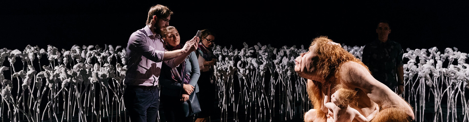
Patricia Piccinini’s Curious Imaginings Courtesy: Vancouver Biennale [downloaded from http://dailyhive.com/vancouver/vancouver-biennale-unsual-public-art-2018/]

Up to this point, I’ve been a little jealous of the Art/Sci Salon’s (Toronto, Canada) January 2018 workshops for artists and discussions about CRISPR ((clustered regularly interspaced short palindromic repeats))/Cas9 and its social implications. (See my January 10, 2018 posting for more about the events.) Now, it seems Vancouver may be in line for its ‘own’ discussion about CRISPR and the implications of gene editing. The image you saw (above) represents one of the installations being hosted by the 2018 – 2020 edition of the Vancouver Biennale.

While this posting is mostly about the Biennale and Piccinini’s work, there is a ‘science’ subsection featuring the science of CRISPR and xenotransplantation. Getting back to the Biennale and Piccinini: A major public art event since 1988, the Vancouver Biennale has hosted over 91 outdoor sculptures and new media works by more than 78 participating artists from over 25 countries and from 4 continents.

Quickie description of the 2018 – 2020 Vancouver Biennale

The latest edition of the Vancouver Biennale was featured in a June 6, 2018 news item on the Daily Hive (Vancouver),

The Vancouver Biennale will be bringing new —and unusual— works of public art to the city beginning this June.

The theme for this season’s Vancouver Biennale exhibition is “re-IMAGE-n” and it kicks off on June 20 [2018] in Vanier Park with Saudi artist Ajlan Gharem’s Paradise Has Many Gates.

Gharem’s architectural chain-link sculpture resembles a traditional mosque, the piece is meant to challenge the notions of religious orthodoxy and encourages individuals to image a space free of Islamophobia.

Melbourne artist Patricia Piccinini’s Curious Imaginings is expected to be one of the most talked about installations of the exhibit. Her style of “oddly captivating, somewhat grotesque, human-animal hybrid creature” is meant to be shocking and thought-provoking.

Piccinini’s interactive [emphasis mine] experience will “challenge us to explore the social impacts of emerging biotechnology and our ethical limits in an age where genetic engineering and digital technologies are already pushing the boundaries of humanity.”

Piccinini’s work will be displayed in the 105-year-old Patricia Hotel in Vancouver’s Strathcona neighbourhood. The 90-day ticketed exhibition [emphasis mine] is scheduled to open this September [2018].

Given that this blog is focused on nanotechnology and other emerging technologies such as CRISPR, I’m focusing on Piccinini’s work and its art/science or sci-art status. This image from the GOMA Gallery where Piccinini’s ‘Curious Affection‘ installation is being shown from March 24 – Aug. 5, 2018 in Brisbane, Queensland, Australia may give you some sense of what one of her installations is like,

Courtesy: Queensland Art Gallery | Gallery of Modern Art (QAGOMA)

I spoke with Serena at the Vancouver Biennale office and asked about the ‘interactive’ aspect of Piccinini’s installation. She suggested the term ‘immersive’ as an alternative. In other words, you won’t be playing with the sculptures or pressing buttons and interacting with computer screens or robots. She also noted that the ticket prices have not been set yet and they are currently developing events focused on the issues raised by the installation. She knew that 2018 is the 200th anniversary of the publication of Mary Shelley’s Frankenstein but I’m not sure how the Biennale folks plan (or don’t plan)  to integrate any recognition of the novle’s impact on the discussions about ‘new’ technologies .They expect Piccinini will visit Vancouver. (Note 1: Piccinini’s work can  also be seen in a group exhibition titled: Frankenstein’s Birthday Party at the Hosfselt Gallery in San Francisco (California, US) from June 23 – August 11, 2018.  Note 2: I featured a number of international events commemorating the 200th anniversary of the publication of Mary Shelley’s novel, Frankenstein, in my Feb. 26, 2018 posting. Note 3: The term ‘Frankenfoods’ helped to shape the discussion of genetically modified organisms and food supply on this planet. It was a wildly successful campaign for activists affecting legislation in some areas of research. Scientists have not been as enthusiastic about the effects. My January 15, 2009 posting briefly traces a history of the term.)

The 2018 – 2020 Vancouver Biennale and science

A June 7, 2018 Vancouver Biennale news release provides more detail about the current series of exhibitions,

The Biennale is also committed to presenting artwork at the cutting edge of discussion and in keeping with the STEAM (science, technology, engineering, arts, math[ematics]) approach to integrating the arts and sciences. In August [2018], Colombian/American visual artist Jessica Angel will present her monumental installation Dogethereum Bridge at Hinge Park in Olympic Village. Inspired by blockchain technology, the artwork’s design was created through the integration of scientific algorithms, new developments in technology, and the arts. This installation, which will serve as an immersive space and collaborative hub for artists and technologists, will host a series of activations with blockchain as the inspirational jumping-off point.

In what is expected to become one of North America’s most talked-about exhibitions of the year, Melbourne artist Patricia Piccinini’s Curious Imaginings will see the intersection of art, science, and ethics. For the first time in the Biennale’s fifteen years of creating transformative experiences, and in keeping with the 2018-2020 theme of “re-IMAGE-n,” the Biennale will explore art in unexpected places by exhibiting in unconventional interior spaces.  The hyperrealist “world of oddly captivating, somewhat grotesque, human-animal hybrid creatures” will be the artist’s first exhibit in a non-museum setting, transforming a wing of the 105-year-old Patricia Hotel. Situated in Vancouver’s oldest neighbourbood of Strathcona, Piccinini’s interactive experience will “challenge us to explore the social impacts of emerging bio-technology and our ethical limits in an age where genetic engineering and digital technologies are already pushing the boundaries of humanity.” In this intimate hotel setting located in a neighborhood continually undergoing its own change, Curious Imaginings will empower visitors to personally consider questions posed by the exhibition, including the promises and consequences of genetic research and human interference. …

There are other pieces being presented at the Biennale but my special interest is in the art/sci pieces and, at this point, CRISPR.

Piccinini in more depth

You can find out more about Patricia Piccinini in her biography on the Vancouver Biennale website but I found this Char Larsson April 7, 2018 article for the Independent (UK) more informative (Note: A link has been removed),

Patricia Piccinini’s sculptures are deeply disquieting. Walking through Curious Affection, her new solo exhibition at Brisbane’s Gallery of Modern Art, is akin to entering a science laboratory full of DNA experiments. Made from silicone, fibreglass and even human hair, her sculptures are breathtakingly lifelike, however, we can’t be sure what life they are like. The artist creates an exuberant parallel universe where transgenic experiments flourish and human evolution has given way to genetic engineering and DNA splicing.

Curious Affection is a timely and welcome recognition of Piccinini’s enormous contribution to reaching back to the mid-1990s. Working across a variety of mediums including photography, video and drawing, she is perhaps best known for her hyperreal creations.

As a genre, hyperrealism depends on the skill of the artist to create the illusion of reality. To be truly successful, it must convince the spectator of its realness. Piccinini acknowledges this demand, but with a delightful twist. The excruciating attention to detail deliberately solicits our desire to look, only to generate unease, as her sculptures are imbued with a fascinating otherness. Part human, part animal, the works are uncannily familiar, but also alarmingly “other”.

Inspired by advances in genetically modified pigs to generate replacement organs for humans [also known as xenotransplantation], we are reminded that Piccinini has always been at the forefront of debates concerning the possibilities of science, technology and DNA cloning. She does so, however, with a warm affection and sense of humour, eschewing the hysterical anxiety frequently accompanying these scientific developments.

Beyond the astonishing level of detail achieved by working with silicon and fibreglass, there is an ethics at work here. Piccinini is asking us not to avert our gaze from the other, and in doing so, to develop empathy and understanding through the encounter.

I encourage anyone who’s interested to read Larsson’s entire piece (April 7, 2018 article).

According to her Wikipedia entry, Piccinini works in a variety of media including video, sound, sculpture, and more. She also has her own website.

Gene editing and xenotransplantation

Sarah Zhang’s June 8, 2018 article for The Atlantic provides a peek at the extraordinary degree of interest and competition in the field of gene editing and CRISPR ((clustered regularly interspaced short palindromic repeats))/Cas9 research (Note: A link has been removed),

China Is Genetically Engineering Monkeys With Brain Disorders

Guoping Feng applied to college the first year that Chinese universities reopened after the Cultural Revolution. It was 1977, and more than a decade’s worth of students—5.7 million—sat for the entrance exams. Feng was the only one in his high school to get in. He was assigned—by chance, essentially—to medical school. Like most of his contemporaries with scientific ambitions, he soon set his sights on graduate studies in the United States. “China was really like 30 to 50 years behind,” he says. “There was no way to do cutting-edge research.” So in 1989, he left for Buffalo, New York, where for the first time he saw snow piled several feet high. He completed his Ph.D. in genetics at the State University of New York at Buffalo.

Feng is short and slim, with a monk-like placidity and a quick smile, and he now holds an endowed chair in neuroscience at MIT, where he focuses on the genetics of brain disorders. His 45-person lab is part of the McGovern Institute for Brain Research, which was established in 2000 with the promise of a $350 million donation, the largest ever received by the university. In short, his lab does not lack for much.

Yet Feng now travels to China several times a year, because there, he can pursue research he has not yet been able to carry out in the United States. [emphasis mine] …

Feng had organized a symposium at SIAT [Shenzhen Institutes of Advanced Technology], and he was not the only scientist who traveled all the way from the United States to attend: He invited several colleagues as symposium speakers, including a fellow MIT neuroscientist interested in tree shrews, a tiny mammal related to primates and native to southern China, and Chinese-born neuroscientists who study addiction at the University of Pittsburgh and SUNY Upstate Medical University. Like Feng, they had left China in the ’80s and ’90s, part of a wave of young scientists in search of better opportunities abroad. Also like Feng, they were back in China to pursue a type of cutting-edge research too expensive and too impractical—and maybe too ethically sensitive—in the United States.

Here’s what precipitated Feng’s work in China, (from Zhang’s article; Note: Links have been removed)

At MIT, Feng’s lab worked on genetically engineering a monkey species called marmosets, which are very small and genuinely bizarre-looking. They are cheaper to keep due to their size, but they are a relatively new lab animal, and they can be difficult to train on lab tasks. For this reason, Feng also wanted to study Shank3 on macaques in China. Scientists have been cataloging the social behavior of macaques for decades, making it an obvious model for studies of disorders like autism that have a strong social component. Macaques are also more closely related to humans than marmosets, making their brains a better stand-in for those of humans.

The process of genetically engineering a macaque is not trivial, even with the advanced tools of CRISPR. Researchers begin by dosing female monkeys with the same hormones used in human in vitro fertilization. They then collect and fertilize the eggs, and inject the resulting embryos with CRISPR proteins using a long, thin glass needle. Monkey embryos are far more sensitive than mice embryos, and can be affected by small changes in the pH of the injection or the concentration of CRISPR proteins. Only some of the embryos will have the desired mutation, and only some will survive once implanted in surrogate mothers. It takes dozens of eggs to get to just one live monkey, so making even a few knockout monkeys required the support of a large breeding colony.

The first Shank3 macaque was born in 2015. Four more soon followed, bringing the total to five.

To visit his research animals, Feng now has to fly 8,000 miles across 12 time zones. It would be a lot more convenient to carry out his macaque research in the United States, of course, but so far, he has not been able to.

He originally inquired about making Shank3 macaques at the New England Primate Research Center, one of eight national primate research centers then funded by the National Institutes of Health in partnership with a local institution (Harvard Medical School, in this case). The center was conveniently located in Southborough, Massachusetts, just 20 miles west of the MIT campus. But in 2013, Harvard decided to shutter the center.

The decision came as a shock to the research community, and it was widely interpreted as a sign of waning interest in primate research in the United States. While the national primate centers have been important hubs of research on HIV, Zika, Ebola, and other diseases, they have also come under intense public scrutiny. Animal-rights groups like the Humane Society of the United States have sent investigators to work undercover in the labs, and the media has reported on monkey deaths in grisly detail. Harvard officially made its decision to close for “financial” reasons. But the announcement also came after the high-profile deaths of four monkeys from improper handling between 2010 and 2012. The deaths sparked a backlash; demonstrators showed up at the gates. The university gave itself two years to wind down their primate work, officially closing the center in 2015.

“They screwed themselves,” Michael Halassa, the MIT neuroscientist who spoke at Feng’s symposium, told me in Shenzhen. Wei-Dong Yao, another one of the speakers, chimed in, noting that just two years later CRISPR has created a new wave of interest in primate research. Yao was one of the researchers at Harvard’s primate center before it closed; he now runs a lab at SUNY Upstate Medical University that uses genetically engineered mouse and human stem cells, and he had come to Shenzhen to talk about restarting his addiction research on primates.

Here’s comes the competition (from Zhang’s article; Note: Links have been removed),

While the U.S. government’s biomedical research budget has been largely flat, both national and local governments in China are eager to raise their international scientific profiles, and they are shoveling money into research. A long-rumored, government-sponsored China Brain Project is supposed to give neuroscience research, and primate models in particular, a big funding boost. Chinese scientists may command larger salaries, too: Thanks to funding from the Shenzhen local government, a new principal investigator returning from overseas can get 3 million yuan—almost half a million U.S. dollars—over his or her first five years. China is even finding success in attracting foreign researchers from top U.S. institutions like Yale.

In the past few years, China has seen a miniature explosion of genetic engineering in monkeys. In Kunming, Shanghai, and Guangzhou, scientists have created monkeys engineered to show signs of Parkinson’s, Duchenne muscular dystrophy, autism, and more. And Feng’s group is not even the only one in China to have created Shank3 monkeys. Another group—a collaboration primarily between researchers at Emory University and scientists in China—has done the same.

Chinese scientists’ enthusiasm for CRISPR also extends to studies of humans, which are moving much more quickly, and in some cases under less oversight, than in the West. The first studies to edit human embryos and first clinical trials for cancer therapies using CRISPR have all happened in China. [emphases mine]

Some ethical issues are also covered (from Zhang’s article),

Parents with severely epileptic children had asked him if it would be possible to study the condition in a monkey. Feng told them what he thought would be technically possible. “But I also said, ‘I’m not sure I want to generate a model like this,’” he recalled. Maybe if there were a drug to control the monkeys’ seizures, he said: “I cannot see them seizure all the time.”

But is it ethical, he continued, to let these babies die without doing anything? Is it ethical to generate thousands or millions of mutant mice for studies of brain disorders, even when you know they will not elucidate much about human conditions?

Primates should only be used if other models do not work, says Feng, and only if a clear path forward is identified. The first step in his work, he says, is to use the Shank3 monkeys to identify the changes the mutations cause in the brain. Then, researchers might use that information to find targets for drugs, which could be tested in the same monkeys. He’s talking with the Oregon National Primate Research Center about carrying out similar work in the United States. ….[Note: I have a three-part series about CRISPR and germline editing* in the US, precipitated by research coming out of Oregon, Part 1, which links to the other parts, is here.]

Zhang’s June 8, 2018 article is excellent and I highly recommend reading it.

I touched on the topic of xenotransplanttaion in a commentary on a book about the science  of the television series, Orphan Black in a January 31,2018 posting (Note: A chimera is what you use to incubate a ‘human’ organ for transplantation or, more accurately, xenotransplantation),

On the subject of chimeras, the Canadian Broadcasting Corporation (CBC) featured a January 26, 2017 article about the pig-human chimeras on its website along with a video,

The end

I am very excited to see Piccinini’s work come to Vancouver. There have been a number of wonderful art and art/science installations and discussions here but this is the first one (I believe) to tackle the emerging gene editing technologies and the issues they raise. (It also fits in rather nicely with the 200th anniversary of the publication of Mary Shelley’s Frankenstein which continues to raise issues and stimulate discussion.)

In addition to the ethical issues raised in Zhang’s article, there are some other philosophical questions:

  • what does it mean to be human
  • if we are going to edit genes to create hybrid human/animals, what are they and how do they fit into our current animal/human schema
  • are you still human if you’ve had an organ transplant where the organ was incubated in a pig

There are also going to be legal issues. In addition to any questions about legal status, there are also fights about intellectual property such as the one involving Harvard & MIT’s [Massachusetts Institute of Technology] Broad Institute vs the University of California at Berkeley (March 15, 2017 posting)..

While I’m thrilled about the Piccinini installation, it should be noted the issues raised by other artworks hosted in this version of the Biennale are important. Happily, they have been broached here in Vancouver before and I suspect this will result in more nuanced  ‘conversations’ than are possible when a ‘new’ issue is introduced.

Bravo 2018 – 2020 Vancouver Biennale!

* Germline editing is when your gene editing will affect subsequent generations as opposed to editing out a mutated gene for the lifetime of a single individual.

Art/sci and CRISPR links

This art/science posting may prove of some interest:

The connectedness of living things: an art/sci project in Saskatchewan: evolutionary biology (February 16, 2018)

A selection of my CRISPR posts:

CRISPR and editing the germline in the US (part 1 of 3): In the beginning (August 15, 2017)

NOTE: An introductory CRISPR video describing how CRISPR/Cas9 works was embedded in part1.

Why don’t you CRISPR yourself? (January 25, 2018)

Editing the genome with CRISPR ((clustered regularly interspaced short palindromic repeats)-carrying nanoparticles (January 26, 2018)

Immune to CRISPR? (April 10, 2018)

3-D integration of nanotechnologies on a single computer chip

By integrating nanomaterials , a new technique for a 3D computer chip capable of handling today’s huge amount of data has been developed. Weirdly, the first two paragraphs of a July 5, 2017 news item on Nanowerk do not convey the main point (Note: A link has been removed),

As embedded intelligence is finding its way into ever more areas of our lives, fields ranging from autonomous driving to personalized medicine are generating huge amounts of data. But just as the flood of data is reaching massive proportions, the ability of computer chips to process it into useful information is stalling.

Now, researchers at Stanford University and MIT have built a new chip to overcome this hurdle. The results are published today in the journal Nature (“Three-dimensional integration of nanotechnologies for computing and data storage on a single chip”), by lead author Max Shulaker, an assistant professor of electrical engineering and computer science at MIT. Shulaker began the work as a PhD student alongside H.-S. Philip Wong and his advisor Subhasish Mitra, professors of electrical engineering and computer science at Stanford. The team also included professors Roger Howe and Krishna Saraswat, also from Stanford.

This image helps to convey the main points,

Instead of relying on silicon-based devices, a new chip uses carbon nanotubes and resistive random-access memory (RRAM) cells. The two are built vertically over one another, making a new, dense 3-D computer architecture with interleaving layers of logic and memory. Courtesy MIT

As I hove been quite impressed with their science writing, it was a bit surprising to find that the Massachusetts Institute of Technology (MIT) had issued this news release (news item) as it didn’t follow the ‘rules’, i.e., cover as many of the journalistic questions (Who, What, Where, When, Why, and, sometimes, How) as possible in the first sentence/paragraph. This is written more in the style of a magazine article and so the details take a while to emerge, from a July 5, 2017 MIT news release, which originated the news item,

Computers today comprise different chips cobbled together. There is a chip for computing and a separate chip for data storage, and the connections between the two are limited. As applications analyze increasingly massive volumes of data, the limited rate at which data can be moved between different chips is creating a critical communication “bottleneck.” And with limited real estate on the chip, there is not enough room to place them side-by-side, even as they have been miniaturized (a phenomenon known as Moore’s Law).

To make matters worse, the underlying devices, transistors made from silicon, are no longer improving at the historic rate that they have for decades.

The new prototype chip is a radical change from today’s chips. It uses multiple nanotechnologies, together with a new computer architecture, to reverse both of these trends.

Instead of relying on silicon-based devices, the chip uses carbon nanotubes, which are sheets of 2-D graphene formed into nanocylinders, and resistive random-access memory (RRAM) cells, a type of nonvolatile memory that operates by changing the resistance of a solid dielectric material. The researchers integrated over 1 million RRAM cells and 2 million carbon nanotube field-effect transistors, making the most complex nanoelectronic system ever made with emerging nanotechnologies.

The RRAM and carbon nanotubes are built vertically over one another, making a new, dense 3-D computer architecture with interleaving layers of logic and memory. By inserting ultradense wires between these layers, this 3-D architecture promises to address the communication bottleneck.

However, such an architecture is not possible with existing silicon-based technology, according to the paper’s lead author, Max Shulaker, who is a core member of MIT’s Microsystems Technology Laboratories. “Circuits today are 2-D, since building conventional silicon transistors involves extremely high temperatures of over 1,000 degrees Celsius,” says Shulaker. “If you then build a second layer of silicon circuits on top, that high temperature will damage the bottom layer of circuits.”

The key in this work is that carbon nanotube circuits and RRAM memory can be fabricated at much lower temperatures, below 200 C. “This means they can be built up in layers without harming the circuits beneath,” Shulaker says.

This provides several simultaneous benefits for future computing systems. “The devices are better: Logic made from carbon nanotubes can be an order of magnitude more energy-efficient compared to today’s logic made from silicon, and similarly, RRAM can be denser, faster, and more energy-efficient compared to DRAM,” Wong says, referring to a conventional memory known as dynamic random-access memory.

“In addition to improved devices, 3-D integration can address another key consideration in systems: the interconnects within and between chips,” Saraswat adds.

“The new 3-D computer architecture provides dense and fine-grained integration of computating and data storage, drastically overcoming the bottleneck from moving data between chips,” Mitra says. “As a result, the chip is able to store massive amounts of data and perform on-chip processing to transform a data deluge into useful information.”

To demonstrate the potential of the technology, the researchers took advantage of the ability of carbon nanotubes to also act as sensors. On the top layer of the chip they placed over 1 million carbon nanotube-based sensors, which they used to detect and classify ambient gases.

Due to the layering of sensing, data storage, and computing, the chip was able to measure each of the sensors in parallel, and then write directly into its memory, generating huge bandwidth, Shulaker says.

Three-dimensional integration is the most promising approach to continue the technology scaling path set forth by Moore’s laws, allowing an increasing number of devices to be integrated per unit volume, according to Jan Rabaey, a professor of electrical engineering and computer science at the University of California at Berkeley, who was not involved in the research.

“It leads to a fundamentally different perspective on computing architectures, enabling an intimate interweaving of memory and logic,” Rabaey says. “These structures may be particularly suited for alternative learning-based computational paradigms such as brain-inspired systems and deep neural nets, and the approach presented by the authors is definitely a great first step in that direction.”

“One big advantage of our demonstration is that it is compatible with today’s silicon infrastructure, both in terms of fabrication and design,” says Howe.

“The fact that this strategy is both CMOS [complementary metal-oxide-semiconductor] compatible and viable for a variety of applications suggests that it is a significant step in the continued advancement of Moore’s Law,” says Ken Hansen, president and CEO of the Semiconductor Research Corporation, which supported the research. “To sustain the promise of Moore’s Law economics, innovative heterogeneous approaches are required as dimensional scaling is no longer sufficient. This pioneering work embodies that philosophy.”

The team is working to improve the underlying nanotechnologies, while exploring the new 3-D computer architecture. For Shulaker, the next step is working with Massachusetts-based semiconductor company Analog Devices to develop new versions of the system that take advantage of its ability to carry out sensing and data processing on the same chip.

So, for example, the devices could be used to detect signs of disease by sensing particular compounds in a patient’s breath, says Shulaker.

“The technology could not only improve traditional computing, but it also opens up a whole new range of applications that we can target,” he says. “My students are now investigating how we can produce chips that do more than just computing.”

“This demonstration of the 3-D integration of sensors, memory, and logic is an exceptionally innovative development that leverages current CMOS technology with the new capabilities of carbon nanotube field–effect transistors,” says Sam Fuller, CTO emeritus of Analog Devices, who was not involved in the research. “This has the potential to be the platform for many revolutionary applications in the future.”

This work was funded by the Defense Advanced Research Projects Agency [DARPA], the National Science Foundation, Semiconductor Research Corporation, STARnet SONIC, and member companies of the Stanford SystemX Alliance.

Here’s a link to and a citation for the paper,

Three-dimensional integration of nanotechnologies for computing and data storage on a single chip by Max M. Shulaker, Gage Hills, Rebecca S. Park, Roger T. Howe, Krishna Saraswat, H.-S. Philip Wong, & Subhasish Mitra. Nature 547, 74–78 (06 July 2017) doi:10.1038/nature22994 Published online 05 July 2017

This paper is behind a paywall.

Shades of the Nokia Morph: a smartphone than conforms to your wrist

A March 16, 2017 news item on Nanowerk brought back some memories for me,

Some day, your smartphone might completely conform to your wrist, and when it does, it might be covered in pure gold, thanks to researchers at Missouri University of Science and Technology.

Nokia, a Finnish telecommunications company, was promoting its idea for a smartphone ‘and more’ that could be worn around your wrist in a concept called the Morph. It was introduced in 2008 at the Museum of Modern Art in New York City (see my March 20, 2010 posting for one of my last updates on this moribund project). Here’s Nokia’s Morph video (almost 6 mins.),

Getting back to the present day, here’s what the Missouri researchers are working on,

An example of a gold foil peeled from single crystal silicon. Reprinted with permission from Naveen Mahenderkar et al., Science [355]:[1203] (2017)

A March 16, 2017 Missouri University of Science and Technology news release, by Greg Katski, which originated the news item, provides more details about this Missouri version (Note: A link has been removed),

Writing in the March 17 [2017] issue of the journal Science, the S&T researchers say they have developed a way to “grow” thin layers of gold on single crystal wafers of silicon, remove the gold foils, and use them as substrates on which to grow other electronic materials. The research team’s discovery could revolutionize wearable or “flexible” technology research, greatly improving the versatility of such electronics in the future.

According to lead researcher Jay A. Switzer, the majority of research into wearable technology has been done using polymer substrates, or substrates made up of multiple crystals. “And then they put some typically organic semiconductor on there that ends up being flexible, but you lose the order that (silicon) has,” says Switzer, Donald L. Castleman/FCR Endowed Professor of Discovery in Chemistry at S&T.

Because the polymer substrates are made up of multiple crystals, they have what are called grain boundaries, says Switzer. These grain boundaries can greatly limit the performance of an electronic device.

“Say you’re making a solar cell or an LED,” he says. “In a semiconductor, you have electrons and you have holes, which are the opposite of electrons. They can combine at grain boundaries and give off heat. And then you end up losing the light that you get out of an LED, or the current or voltage that you might get out of a solar cell.”

Most electronics on the market are made of silicon because it’s “relatively cheap, but also highly ordered,” Switzer says.

“99.99 percent of electronics are made out of silicon, and there’s a reason – it works great,” he says. “It’s a single crystal, and the atoms are perfectly aligned. But, when you have a single crystal like that, typically, it’s not flexible.”

By starting with single crystal silicon and growing gold foils on it, Switzer is able to keep the high order of silicon on the foil. But because the foil is gold, it’s also highly durable and flexible.

“We bent it 4,000 times, and basically the resistance didn’t change,” he says.

The gold foils are also essentially transparent because they are so thin. According to Switzer, his team has peeled foils as thin as seven nanometers.

Switzer says the challenge his research team faced was not in growing gold on the single crystal silicon, but getting it to peel off as such a thin layer of foil. Gold typically bonds very well to silicon.

“So we came up with this trick where we could photo-electrochemically oxidize the silicon,” Switzer says. “And the gold just slides off.”

Photoelectrochemical oxidation is the process by which light enables a semiconductor material, in this case silicon, to promote a catalytic oxidation reaction.

Switzer says thousands of gold foils—or foils of any number of other metals—can be made from a single crystal wafer of silicon.

The research team’s discovery can be considered a “happy accident.” Switzer says they were looking for a cheap way to make single crystals when they discovered this process.

“This is something that I think a lot of people who are interested in working with highly ordered materials like single crystals would appreciate making really easily,” he says. “Besides making flexible devices, it’s just going to open up a field for anybody who wants to work with single crystals.”

Here’s a link to and a citation for the paper,

Epitaxial lift-off of electrodeposited single-crystal gold foils for flexible electronics by Naveen K. Mahenderkar, Qingzhi Chen, Ying-Chau Liu, Alexander R. Duchild, Seth Hofheins, Eric Chason, Jay A. Switzer. Science  17 Mar 2017: Vol. 355, Issue 6330, pp. 1203-1206 DOI: 10.1126/science.aam5830

This paper is behind a paywall.