Researchers have been working on ways to harvest energy from bloodstreams. I last wrote about this type of research in an April 3, 2009 posting about ‘vampire batteries ‘(for use in pacemakers). The latest work according to a Sept. 8, 2017 news item on Nanowerk comes from China,
Men build dams and huge turbines to turn the energy of waterfalls and tides into electricity. To produce hydropower on a much smaller scale, Chinese scientists have now developed a lightweight power generator based on carbon nanotube fibers suitable to convert even the energy of flowing blood in blood vessels into electricity. They describe their innovation in the journal Angewandte Chemie (“A One-Dimensional Fluidic Nanogenerator with a High Power Conversion Efficiency”)
For thousands of years, people have used the energy of flowing or falling water for their purposes, first to power mechanical engines such as watermills, then to generate electricity by exploiting height differences in the landscape or sea tides. Using naturally flowing water as a sustainable power source has the advantage that there are (almost) no dependencies on weather or daylight. Even flexible, minute power generators that make use of the flow of biological fluids are conceivable. How such a system could work is explained by a research team from Fudan University in Shanghai, China. Huisheng Peng and his co-workers have developed a fiber with a thickness of less than a millimeter that generates electrical power when surrounded by flowing saline solution—in a thin tube or even in a blood vessel.
The construction principle of the fiber is quite simple. An ordered array of carbon nanotubes was continuously wrapped around a polymeric core. Carbon nanotubes are well known to be electroactive and mechanically stable; they can be spun and aligned in sheets. In the as-prepared electroactive threads, the carbon nanotube sheets coated the fiber core with a thickness of less than half a micron. For power generation, the thread or “fiber-shaped fluidic nanogenerator” (FFNG), as the authors call it, was connected to electrodes and immersed into flowing water or simply repeatedly dipped into a saline solution. “The electricity was derived from the relative movement between the FFNG and the solution,” the scientists explained. According to the theory, an electrical double layer is created around the fiber, and then the flowing solution distorts the symmetrical charge distribution, generating an electricity gradient along the long axis.
The power output efficiency of this system was high. Compared with other types of miniature energy-harvesting devices, the FFNG was reported to show a superior power conversion efficiency of more than 20%. Other advantages are elasticity, tunability, lightweight, and one-dimensionality, thus offering prospects of exciting technological applications. The FFNG can be made stretchable just by spinning the sheets around an elastic fiber substrate. If woven into fabrics, wearable electronics become thus a very interesting option for FFNG application. Another exciting application is the harvesting of electrical energy from the bloodstream for medical applications. First tests with frog nerves proved to be successful.
Here’s a link to and a citation for the paper,
A One-Dimensional Fluidic Nanogenerator with a High Power Conversion Efficiency by Yifan Xu, Dr. Peining Chen, Jing Zhang, Songlin Xie, Dr. Fang Wan, Jue Deng, Dr. Xunliang Cheng, Yajie Hu, Meng Liao, Dr. Bingjie Wang, Dr. Xuemei Sun, and Prof. Dr. Huisheng Peng. Angewandte Chemie International Edition DOI: 10.1002/anie.201706620 Version of Record online: 7 SEP 2017
In discussions about water desalination and carbon nanomaterials, it’s graphene that’s usually mentioned these days. By contrast, scientists from the US Department of Energy’s Lawrence Livermore National Laboratory (LLNL) have turned to carbon nanotubes,
There are two news items about the work at LLNL on ScienceDaily, this first one originated by the American Association for the Advancement of Science (AAAS) offers a succinct summary of the work (from an August 24, 2017 news item on ScienceDaily,
At just the right size, carbon nanotubes can filter water with better efficiency than biological proteins, a new study reveals. The results could pave the way to new water filtration systems, at a time when demands for fresh water pose a global threat to sustainable development.
A class of biological proteins, called aquaporins, is able to effectively filter water, yet scientists have not been able to manufacture scalable systems that mimic this ability. Aquaporins usually exhibit channels for filtering water molecules at a narrow width of 0.3 nanometers, which forces the water molecules into a single-file chain.
Here, Ramya H. Tunuguntla and colleagues experimented with nanotubes of different widths to see which ones are best for filtering water. Intriguingly, they found that carbon nanotubes with a width of 0.8 nanometers outperformed aquaporins in filtering efficiency by a factor of six.
These narrow carbon nanotube porins (nCNTPs) were still slim enough to force the water molecules into a single-file chain. The researchers attribute the differences between aquaporins and nCNTPS to differences in hydrogen bonding — whereas pore-lining residues in aquaporins can donate or accept H bonds to incoming water molecules, the walls of CNTPs cannot form H bonds, permitting unimpeded water flow.
The nCNTPs in this study maintained permeability exceeding that of typical saltwater, only diminishing at very high salt concentrations. Lastly, the team found that by changing the charges at the mouth of the nanotube, they can alter the ion selectivity. This advancement is highlighted in a Perspective [in Science magazine] by Zuzanna Siwy and Francesco Fornasiero.
Lawrence Livermore scientists, in collaboration with researchers at Northeastern University, have developed carbon nanotube pores that can exclude salt from seawater. The team also found that water permeability in carbon nanotubes (CNTs) with diameters smaller than a nanometer (0.8 nm) exceeds that of wider carbon nanotubes by an order of magnitude.
The nanotubes, hollow structures made of carbon atoms in a unique arrangement, are more than 50,000 times thinner than a human hair. The super smooth inner surface of the nanotube is responsible for their remarkably high water permeability, while the tiny pore size blocks larger salt ions.
There’s a rather lovely illustration for this work,
An artist’s depiction of the promise of carbon nanotube porins for desalination. The image depicts a stylized carbon nanotube pipe that delivers clean desalinated water from the ocean to a kitchen tap. Image by Ryan Chen/LLNL
Increasing demands for fresh water pose a global threat to sustainable development, resulting in water scarcity for 4 billion people. Current water purification technologies can benefit from the development of membranes with specialized pores that mimic highly efficient and water selective biological proteins.
“We found that carbon nanotubes with diameters smaller than a nanometer bear a key structural feature that enables enhanced transport. The narrow hydrophobic channel forces water to translocate in a single-file arrangement, a phenomenon similar to that found in the most efficient biological water transporters,” said Ramya Tunuguntla, an LLNL postdoctoral researcher and co-author of the manuscript appearing in the Aug. 24 [2017]edition of Science.
Computer simulations and experimental studies of water transport through CNTs with diameters larger than 1 nm showed enhanced water flow, but did not match the transport efficiency of biological proteins and did not separate salt efficiently, especially at higher salinities. The key breakthrough achieved by the LLNL team was to use smaller-diameter nanotubes that delivered the required boost in performance.
“These studies revealed the details of the water transport mechanism and showed that rational manipulation of these parameters can enhance pore efficiency,” said Meni Wanunu, a physics professor at Northeastern University and co-author on the study.
“Carbon nanotubes are a unique platform for studying molecular transport and nanofluidics,” said Alex Noy, LLNL principal investigator on the CNT project and a senior author on the paper. “Their sub-nanometer size, atomically smooth surfaces and similarity to cellular water transport channels make them exceptionally suited for this purpose, and it is very exciting to make a synthetic water channel that performs better than nature’s own.”
This discovery by the LLNL scientists and their colleagues has clear implications for the next generation of water purification technologies and will spur a renewed interest in development of the next generation of high-flux membranes.
Earth is 70 percent water, but only a tiny portion—0.007 percent—is available to drink.
As potable water sources dwindle, global population increases every year. One potential solution to quenching the planet’s thirst is through desalinization—the process of removing salt from seawater. While tantalizing, this approach has always been too expensive and energy intensive for large-scale feasibility.
Now, researchers from Northeastern have made a discovery that could change that, making desalinization easier, faster and cheaper than ever before. In a paper published Thursday [August 24, 2017] in Science, the group describes how carbon nanotubes of a certain size act as the perfect filter for salt—the smallest and most abundant water contaminant.
Filtering water is tricky because water molecules want to stick together. The “H” in H2O is hydrogen, and hydrogen bonds are strong, requiring a lot of energy to separate. Water tends to bulk up and resist being filtered. But nanotubes do it rapidly, with ease.
A carbon nanotube is like an impossibly small rolled up sheet of paper, about a nanometer in diameter. For comparison, the diameter of a human hair is 50 to 70 micrometers—50,000 times wider. The tube’s miniscule size, exactly 0.8 nm, only allows one water molecule to pass through at a time. This single-file lineup disrupts the hydrogen bonds, so water can be pushed through the tubes at an accelerated pace, with no bulking.
“You can imagine if you’re a group of people trying to run through the hallway holding hands, it’s going to be a lot slower than running through the hallway single-file,” said co-author Meni Wanunu, associate professor of physics at Northeastern. Wanunu and post doctoral student Robert Henley collaborated with scientists at the Lawrence Livermore National Laboratory in California to conduct the research.
Scientists led by Aleksandr Noy at Lawrence Livermore discovered last year [2016] that carbon nanotubes were an ideal channel for proton transport. For this new study, Henley brought expertise and technology from Wanunu’s Nanoscale Biophysics Lab to Noy’s lab, and together they took the research one step further.
In addition to being precisely the right size for passing single water molecules, carbon nanotubes have a negative electric charge. This causes them to reject anything with the same charge, like the negative ions in salt, as well as other unwanted particles.
“While salt has a hard time passing through because of the charge, water is a neutral molecule and passes through easily,” Wanunu said. Scientists in Noy’s lab had theorized that carbon nanotubes could be designed for specific ion selectivity, but they didn’t have a reliable system of measurement. Luckily, “That’s the bread and butter of what we do in Meni’s lab,” Henley said. “It created a nice symbiotic relationship.”
“Robert brought the cutting-edge measurement and design capabilities of Wanunu’s group to my lab, and he was indispensable in developing a new platform that we used to measure the ion selectivity of the nanotubes,” Noy said.
The result is a novel system that could have major implications for the future of water security. The study showed that carbon nanotubes are better at desalinization than any other existing method— natural or man-made.
To keep their momentum going, the two labs have partnered with a leading water purification organization based in Israel. And the group was recently awarded a National Science Foundation/Binational Science Foundation grant to conduct further studies and develop water filtration platforms based on their new method. As they continue the research, the researchers hope to start programs where students can learn the latest on water filtration technology—with the goal of increasing that 0.007 percent.
As is usual in these cases there’s a fair degree of repetition but there’s always at least one nugget of new information, in this case, a link to Israel. As I noted many times, the Middle East is experiencing serious water issues. My most recent ‘water and the Middle East’ piece is an August 21, 2017 post about rainmaking at the Masdar Institute in United Arab Emirates. Approximately 50% of the way down the posting, I mention Israel and Palestine’s conflict over water.
The researchers involved in this work are confident enough about their prospects that they will be patenting their research into yarns. From an August 25, 2017 news item on Nanowerk,
An international research team led by scientists at The University of Texas at Dallas and Hanyang University in South Korea has developed high-tech yarns that generate electricity when they are stretched or twisted.
In a study published in the Aug. 25 [2017] issue of the journal Science (“Harvesting electrical energy from carbon nanotube yarn twist”), researchers describe “twistron” yarns and their possible applications, such as harvesting energy from the motion of ocean waves or from temperature fluctuations. When sewn into a shirt, these yarns served as a self-powered breathing monitor.
“The easiest way to think of twistron harvesters is, you have a piece of yarn, you stretch it, and out comes electricity,” said Dr. Carter Haines, associate research professor in the Alan G. MacDiarmid NanoTech Institute at UT Dallas and co-lead author of the article. The article also includes researchers from South Korea, Virginia Tech, Wright-Patterson Air Force Base and China.
The yarns are constructed from carbon nanotubes, which are hollow cylinders of carbon 10,000 times smaller in diameter than a human hair. The researchers first twist-spun the nanotubes into high-strength, lightweight yarns. To make the yarns highly elastic, they introduced so much twist that the yarns coiled like an over-twisted rubber band.
In order to generate electricity, the yarns must be either submerged in or coated with an ionically conducting material, or electrolyte, which can be as simple as a mixture of ordinary table salt and water.
“Fundamentally, these yarns are supercapacitors,” said Dr. Na Li, a research scientist at the NanoTech Institute and co-lead author of the study. “In a normal capacitor, you use energy — like from a battery — to add charges to the capacitor. But in our case, when you insert the carbon nanotube yarn into an electrolyte bath, the yarns are charged by the electrolyte itself. No external battery, or voltage, is needed.”
When a harvester yarn is twisted or stretched, the volume of the carbon nanotube yarn decreases, bringing the electric charges on the yarn closer together and increasing their energy, Haines said. This increases the voltage associated with the charge stored in the yarn, enabling the harvesting of electricity.
Stretching the coiled twistron yarns 30 times a second generated 250 watts per kilogram of peak electrical power when normalized to the harvester’s weight, said Dr. Ray Baughman, director of the NanoTech Institute and a corresponding author of the study.
“Although numerous alternative harvesters have been investigated for many decades, no other reported harvester provides such high electrical power or energy output per cycle as ours for stretching rates between a few cycles per second and 600 cycles per second.”
Lab Tests Show Potential Applications
In the lab, the researchers showed that a twistron yarn weighing less than a housefly could power a small LED, which lit up each time the yarn was stretched.
To show that twistrons can harvest waste thermal energy from the environment, Li connected a twistron yarn to a polymer artificial muscle that contracts and expands when heated and cooled. The twistron harvester converted the mechanical energy generated by the polymer muscle to electrical energy.
“There is a lot of interest in using waste energy to power the Internet of Things, such as arrays of distributed sensors,” Li said. “Twistron technology might be exploited for such applications where changing batteries is impractical.”
The researchers also sewed twistron harvesters into a shirt. Normal breathing stretched the yarn and generated an electrical signal, demonstrating its potential as a self-powered respiration sensor.
“Electronic textiles are of major commercial interest, but how are you going to power them?” Baughman said. “Harvesting electrical energy from human motion is one strategy for eliminating the need for batteries. Our yarns produced over a hundred times higher electrical power per weight when stretched compared to other weavable fibers reported in the literature.”
Electricity from Ocean Waves
“In the lab we showed that our energy harvesters worked using a solution of table salt as the electrolyte,” said Baughman, who holds the Robert A. Welch Distinguished Chair in Chemistry in the School of Natural Sciences and Mathematics. “But we wanted to show that they would also work in ocean water, which is chemically more complex.”
In a proof-of-concept demonstration, co-lead author Dr. Shi Hyeong Kim, a postdoctoral researcher at the NanoTech Institute, waded into the frigid surf off the east coast of South Korea to deploy a coiled twistron in the sea. He attached a 10 centimeter-long yarn, weighing only 1 milligram (about the weight of a mosquito), between a balloon and a sinker that rested on the seabed.
Every time an ocean wave arrived, the balloon would rise, stretching the yarn up to 25 percent, thereby generating measured electricity.
Even though the investigators used very small amounts of twistron yarn in the current study, they have shown that harvester performance is scalable, both by increasing twistron diameter and by operating many yarns in parallel.
“If our twistron harvesters could be made less expensively, they might ultimately be able to harvest the enormous amount of energy available from ocean waves,” Baughman said. “However, at present these harvesters are most suitable for powering sensors and sensor communications. Based on demonstrated average power output, just 31 milligrams of carbon nanotube yarn harvester could provide the electrical energy needed to transmit a 2-kilobyte packet of data over a 100-meter radius every 10 seconds for the Internet of Things.”
The investigators have filed a patent on the technology.
In the U.S., the research was funded by the Air Force, the Air Force Office of Scientific Research, NASA, the Office of Naval Research and the Robert A. Welch Foundation. In Korea, the research was supported by the Korea-U.S. Air Force Cooperation Program and the Creative Research Initiative Center for Self-powered Actuation of the National Research Foundation and the Ministry of Science.
Here’s a link to and a citation for the paper,
Harvesting electrical energy from carbon nanotube yarn twist by Shi Hyeong Kim, Carter S. Haines, Na Li, Keon Jung Kim, Tae Jin Mun, Changsoon Choi, Jiangtao Di, Young Jun Oh, Juan Pablo Oviedo, Julia Bykova, Shaoli Fang, Nan Jiang, Zunfeng Liu, Run Wang, Prashant Kumar, Rui Qiao, Shashank Priya, Kyeongjae Cho, Moon Kim, Matthew Steven Lucas, Lawrence F. Drummy, Benji Maruyama, Dong Youn Lee, Xavier Lepró, Enlai Gao, Dawood Albarq, Raquel Ovalle-Robles, Seon Jeong Kim, Ray H. Baughman. Science 25 Aug 2017: Vol. 357, Issue 6353, pp. 773-778 DOI: 10.1126/science.aam8771
This paper is behind a paywall.
Dexter Johnson in an Aug. 25, 2017 posting on his Nanoclast blog (on the IEEE [Institute of Electrical and Electronics Engineers] website) delves further into the research,
…
“Basically what’s happening is when we stretch the yarn, we’re getting a change in capacitance of the yarn. It’s that change that allows us to get energy out,” explains Carter Haines, associate research professor at UT Dallas and co-lead author of the paper describing the research, in an interview with IEEE Spectrum.
This makes it similar in many ways to other types of energy harvesters. For instance, in other research, it has been demonstrated—with sheets of rubber with coated electrodes on both sides—that you can increase the capacitance of a material when you stretch it and it becomes thinner. As a result, if you have charge on that capacitor, you can change the voltage associated with that charge.
“We’re more or less exploiting the same effect but what we’re doing differently is we’re using an electric chemical cell to do this,” says Haines. “So we’re not changing double layer capacitance in normal parallel plate capacitors. But we’re actually changing the electric chemical capacitance on the surface of a super capacitor yarn.”
While there are other capacitance-based energy harvesters, those other devices require extremely high voltages to work because they’re using parallel plate capacitors, according to Haines.
…
Dexter asks good questions and his post is very informative.
… researchers in Italy and the UK have found a way to make Spidey’s silk a lot stronger, using various different spider species and carbon nanotubes or graphene.
The research team, led by Professor Nicola Pugno at the University of Trento, Italy, succeeded in having their spiders produce silk with up to three times the strength and ten times the toughness of the regular material.
Their discovery, published today in the journal 2D Materials, could pave the way for a new class of bionicomposites, with a wide variety of uses.
Professor Pugno said: “Humans have used silkworm silks widely for thousands of years, but recently research has focussed on spider silk, as it has extremely promising mechanical properties. It is among the best spun polymer fibres in terms of tensile strength, ultimate strain, and especially toughness, even when compared to synthetic fibres such as Kevlar.
“We already know that there are biominerals present in in the protein matrices and hard tissues of insects, which gives them high strength and hardness in their jaws, mandibles and teeth, for example. So our study looked at whether spider silk’s properties could be ‘enhanced’ by artificially incorporating various different nanomaterials into the silk’s biological protein structures.”
To do this, the team exposed three different spider species to water dispersions containing carbon nanotubes or graphene.
After collecting the spiders’ silk, the team tested its tensile strength and toughness.
Professor Pugno said: “We found that the strongest silk the spiders spun had a fracture strength up to 5.4 gigapascals (GPa), and a toughness modulus up to 1,570 joules per gram (J/g). Normal spider silk, by comparison, has a fracture strength of around 1.5 GPa and a toughness modulus of around 150 J/g.
“This is the highest fibre toughness discovered to date, and a strength comparable to that of the strongest carbon fibres or limpet teeth. These are still early days, but our results are a proof of concept that paves the way to exploiting the naturally efficient spider spinning process to produce reinforced bionic silk fibres, thus further improving one of the most promising strong materials.
“These silks’ high toughness and resistance to ultimate strain could have applications such as parachutes.”
“Furthermore, this process of the natural integration of reinforcements in biological structural materials could also be applied to other animals and plants, leading to a new class of “bionicomposites” for innovative applications.”
Remember this? “You are what you eat.” If you’ve ever had doubts about that saying, these spiders should be laying them to rest.
Sadly, this news release doesn’t explain much about the decision to feed the spiders graphene or carbon nanotubes, which are identical other than in their respective shapes (sheet vs tube) and whether those shapes did or did not affect the strength of the silk.
Here’s a link to and a citation for the paper,
Spider silk reinforced by graphene or carbon nanotubes by Emiliano Lepore, Federico Bosia, Francesco Bonaccorso, Matteo Bruna, Simone Taioli, Giovanni Garberoglio, Andrea C Ferrari, and Nicola Maria Pugno. 2D Materials, Volume 4, Number 3 DOI: https://doi.org/10.1088/2053-1583/aa7cd3 Published 14 August 2017
Pugno was most recently mentioned here in a May 29, 2015 posting where he was listed as an author for a paper on synthesizing spider silk. Prior to 2015 I was familiar with Pugno’s name due to his work on adhesiveness in geckos.
By integrating nanomaterials , a new technique for a 3D computer chip capable of handling today’s huge amount of data has been developed. Weirdly, the first two paragraphs of a July 5, 2017 news item on Nanowerk do not convey the main point (Note: A link has been removed),
As embedded intelligence is finding its way into ever more areas of our lives, fields ranging from autonomous driving to personalized medicine are generating huge amounts of data. But just as the flood of data is reaching massive proportions, the ability of computer chips to process it into useful information is stalling.
Now, researchers at Stanford University and MIT have built a new chip to overcome this hurdle. The results are published today in the journal Nature (“Three-dimensional integration of nanotechnologies for computing and data storage on a single chip”), by lead author Max Shulaker, an assistant professor of electrical engineering and computer science at MIT. Shulaker began the work as a PhD student alongside H.-S. Philip Wong and his advisor Subhasish Mitra, professors of electrical engineering and computer science at Stanford. The team also included professors Roger Howe and Krishna Saraswat, also from Stanford.
This image helps to convey the main points,
Instead of relying on silicon-based devices, a new chip uses carbon nanotubes and resistive random-access memory (RRAM) cells. The two are built vertically over one another, making a new, dense 3-D computer architecture with interleaving layers of logic and memory. Courtesy MIT
As I hove been quite impressed with their science writing, it was a bit surprising to find that the Massachusetts Institute of Technology (MIT) had issued this news release (news item) as it didn’t follow the ‘rules’, i.e., cover as many of the journalistic questions (Who, What, Where, When, Why, and, sometimes, How) as possible in the first sentence/paragraph. This is written more in the style of a magazine article and so the details take a while to emerge, from a July 5, 2017 MIT news release, which originated the news item,
Computers today comprise different chips cobbled together. There is a chip for computing and a separate chip for data storage, and the connections between the two are limited. As applications analyze increasingly massive volumes of data, the limited rate at which data can be moved between different chips is creating a critical communication “bottleneck.” And with limited real estate on the chip, there is not enough room to place them side-by-side, even as they have been miniaturized (a phenomenon known as Moore’s Law).
To make matters worse, the underlying devices, transistors made from silicon, are no longer improving at the historic rate that they have for decades.
The new prototype chip is a radical change from today’s chips. It uses multiple nanotechnologies, together with a new computer architecture, to reverse both of these trends.
Instead of relying on silicon-based devices, the chip uses carbon nanotubes, which are sheets of 2-D graphene formed into nanocylinders, and resistive random-access memory (RRAM) cells, a type of nonvolatile memory that operates by changing the resistance of a solid dielectric material. The researchers integrated over 1 million RRAM cells and 2 million carbon nanotube field-effect transistors, making the most complex nanoelectronic system ever made with emerging nanotechnologies.
The RRAM and carbon nanotubes are built vertically over one another, making a new, dense 3-D computer architecture with interleaving layers of logic and memory. By inserting ultradense wires between these layers, this 3-D architecture promises to address the communication bottleneck.
However, such an architecture is not possible with existing silicon-based technology, according to the paper’s lead author, Max Shulaker, who is a core member of MIT’s Microsystems Technology Laboratories. “Circuits today are 2-D, since building conventional silicon transistors involves extremely high temperatures of over 1,000 degrees Celsius,” says Shulaker. “If you then build a second layer of silicon circuits on top, that high temperature will damage the bottom layer of circuits.”
The key in this work is that carbon nanotube circuits and RRAM memory can be fabricated at much lower temperatures, below 200 C. “This means they can be built up in layers without harming the circuits beneath,” Shulaker says.
This provides several simultaneous benefits for future computing systems. “The devices are better: Logic made from carbon nanotubes can be an order of magnitude more energy-efficient compared to today’s logic made from silicon, and similarly, RRAM can be denser, faster, and more energy-efficient compared to DRAM,” Wong says, referring to a conventional memory known as dynamic random-access memory.
“In addition to improved devices, 3-D integration can address another key consideration in systems: the interconnects within and between chips,” Saraswat adds.
“The new 3-D computer architecture provides dense and fine-grained integration of computating and data storage, drastically overcoming the bottleneck from moving data between chips,” Mitra says. “As a result, the chip is able to store massive amounts of data and perform on-chip processing to transform a data deluge into useful information.”
To demonstrate the potential of the technology, the researchers took advantage of the ability of carbon nanotubes to also act as sensors. On the top layer of the chip they placed over 1 million carbon nanotube-based sensors, which they used to detect and classify ambient gases.
Due to the layering of sensing, data storage, and computing, the chip was able to measure each of the sensors in parallel, and then write directly into its memory, generating huge bandwidth, Shulaker says.
Three-dimensional integration is the most promising approach to continue the technology scaling path set forth by Moore’s laws, allowing an increasing number of devices to be integrated per unit volume, according to Jan Rabaey, a professor of electrical engineering and computer science at the University of California at Berkeley, who was not involved in the research.
“It leads to a fundamentally different perspective on computing architectures, enabling an intimate interweaving of memory and logic,” Rabaey says. “These structures may be particularly suited for alternative learning-based computational paradigms such as brain-inspired systems and deep neural nets, and the approach presented by the authors is definitely a great first step in that direction.”
“One big advantage of our demonstration is that it is compatible with today’s silicon infrastructure, both in terms of fabrication and design,” says Howe.
“The fact that this strategy is both CMOS [complementary metal-oxide-semiconductor] compatible and viable for a variety of applications suggests that it is a significant step in the continued advancement of Moore’s Law,” says Ken Hansen, president and CEO of the Semiconductor Research Corporation, which supported the research. “To sustain the promise of Moore’s Law economics, innovative heterogeneous approaches are required as dimensional scaling is no longer sufficient. This pioneering work embodies that philosophy.”
The team is working to improve the underlying nanotechnologies, while exploring the new 3-D computer architecture. For Shulaker, the next step is working with Massachusetts-based semiconductor company Analog Devices to develop new versions of the system that take advantage of its ability to carry out sensing and data processing on the same chip.
So, for example, the devices could be used to detect signs of disease by sensing particular compounds in a patient’s breath, says Shulaker.
“The technology could not only improve traditional computing, but it also opens up a whole new range of applications that we can target,” he says. “My students are now investigating how we can produce chips that do more than just computing.”
“This demonstration of the 3-D integration of sensors, memory, and logic is an exceptionally innovative development that leverages current CMOS technology with the new capabilities of carbon nanotube field–effect transistors,” says Sam Fuller, CTO emeritus of Analog Devices, who was not involved in the research. “This has the potential to be the platform for many revolutionary applications in the future.”
This work was funded by the Defense Advanced Research Projects Agency [DARPA], the National Science Foundation, Semiconductor Research Corporation, STARnet SONIC, and member companies of the Stanford SystemX Alliance.
Can cyborg brains be far behind now that researchers are looking at ways to repair nerve fibers with carbon nanotubes (CNTs)? A June 26, 2017 news item on ScienceDaily describes the scheme using carbon nanotubes as a material for repairing nerve fibers,
Carbon nanotubes exhibit interesting characteristics rendering them particularly suited to the construction of special hybrid devices — consisting of biological issue and synthetic material — planned to re-establish connections between nerve cells, for instance at spinal level, lost on account of lesions or trauma. This is the result of a piece of research published on the scientific journal Nanomedicine: Nanotechnology, Biology, and Medicine conducted by a multi-disciplinary team comprising SISSA (International School for Advanced Studies), the University of Trieste, ELETTRA Sincrotrone and two Spanish institutions, Basque Foundation for Science and CIC BiomaGUNE. More specifically, researchers have investigated the possible effects on neurons of the interaction with carbon nanotubes. Scientists have proven that these nanomaterials may regulate the formation of synapses, specialized structures through which the nerve cells communicate, and modulate biological mechanisms, such as the growth of neurons, as part of a self-regulating process. This result, which shows the extent to which the integration between nerve cells and these synthetic structures is stable and efficient, highlights the great potentialities of carbon nanotubes as innovative materials capable of facilitating neuronal regeneration or in order to create a kind of artificial bridge between groups of neurons whose connection has been interrupted. In vivo testing has actually already begun.
The researchers have included a gorgeous image to illustrate their work,
Caption: Scientists have proven that these nanomaterials may regulate the formation of synapses, specialized structures through which the nerve cells communicate, and modulate biological mechanisms, such as the growth of neurons, as part of a self-regulating process. Credit: Pixabay
“Interface systems, or, more in general, neuronal prostheses, that enable an effective re-establishment of these connections are under active investigation” explain Laura Ballerini (SISSA) and Maurizio Prato (UniTS-CIC BiomaGUNE), coordinating the research project. “The perfect material to build these neural interfaces does not exist, yet the carbon nanotubes we are working on have already proved to have great potentialities. After all, nanomaterials currently represent our best hope for developing innovative strategies in the treatment of spinal cord injuries”. These nanomaterials are used both as scaffolds, a supportive framework for nerve cells, and as means of interfaces releasing those signals that empower nerve cells to communicate with each other.
Many aspects, however, still need to be addressed. Among them, the impact on neuronal physiology of the integration of these nanometric structures with the cell membrane. “Studying the interaction between these two elements is crucial, as it might also lead to some undesired effects, which we ought to exclude”. Laura Ballerini explains: “If, for example, the mere contact provoked a vertiginous rise in the number of synapses, these materials would be essentially unusable”. “This”, Maurizio Prato adds, “is precisely what we have investigated in this study where we used pure carbon nanotubes”.
The results of the research are extremely encouraging: “First of all we have proved that nanotubes do not interfere with the composition of lipids, of cholesterol in particular, which make up the cellular membrane in neurons. Membrane lipids play a very important role in the transmission of signals through the synapses. Nanotubes do not seem to influence this process, which is very important”.
There is more, however. The research has also highlighted the fact that the nerve cells growing on the substratum of nanotubes, thanks to this interaction, develop and reach maturity very quickly, eventually reaching a condition of biological homeostasis. “Nanotubes facilitate the full growth of neurons and the formation of new synapses. This growth, however, is not indiscriminate and unlimited since, as we proved, after a few weeks a physiological balance is attained. Having established the fact that this interaction is stable and efficient is an aspect of fundamental importance”. Maurizio Prato and Laura Ballerini conclude as follows: “We are proving that carbon nanotubes perform excellently in terms of duration, adaptability and mechanical compatibility with the tissue. Now we know that their interaction with the biological material, too, is efficient. Based on this evidence, we are already studying the in vivo application, and preliminary results appear to be quite promising also in terms of recovery of the lost neurological functions”.
This desalination technology comes from the United Arab Emirates (UAE). from an April 13, 2017 news item on Nanowerk,
An advanced water treatment membrane made of electrically conductive nanofibers developed at Masdar Institute was highlighted by Dr. Raed Hashaikeh, Professor of Mechanical and Materials Engineering at Masdar Institute, in his keynote speech during the 3rd International Conference on Desalination using Membrane Technology held last week in Spain.
Self-cleaning membranes offer a critically needed solution to the problem of fouling, which is the unwanted build-up of organic and inorganic deposits on a membrane’s surface that reduces the membrane’s ability to filter impurities. Water treatment and purification membranes that can easily clean themselves when fouled could make pressure-driven membrane filtration systems used to treat and desalinate water more energy-efficient.
“Keeping membranes clean, permeable and functional is a great challenge to membrane desalination technologies. When a membrane becomes fouled, its pores get blocked and its flux is severely reduced, which means that much less water can pass through the membrane at a constant pressure,” Dr. Hashaikeh explained.
Conventional methods for cleaning fouled membranes involve expensive and harsh chemical treatments, and often lead to water treatment plant shut-downs, which can cost millions of dollars in lost operational hours. In the UAE, annual spending on desalination is already estimated to cost AED12 billion, indicating a pressing need for solutions that avoid costly shut-downs and treatments.
In addition to posing a heavy financial burden, fouled membranes are also a sustainability issue, as once a membrane becomes fouled, the higher pressure needed to push water through clogged pores significantly increases the plant’s energy consumption. The harsh chemicals used to clean a fouled membrane are also bad for the environment and require neutralizing. Thus, finding a way to easily and quickly clean fouled membranes not only makes financial sense, but environmental sense.
In a country like the UAE, where natural gas-powered thermal desalination produces over 80% of the country’s domestic water, innovative technologies like self-cleaning membranes to support a shift toward lower-energy and lower-cost membrane-based desalination are essential for achieving economic and environmental balance while meeting the UAE’s water demands.
And now, Dr. Hashaikeh’s research group may have brought the UAE closer towards realizing a more sustainable and economic approach to membrane desalination through their research on the application of advanced nanofibers for enhanced, self-cleaning membranes.
The group has leveraged the electrically conductive nature of a special kind of nanofiber, called carbon nanotubes (CNT). CNTs are tiny cylindrical tubes made of tightly bonded carbon atoms, measuring just one atom thick. But the CNTs Dr. Hashaikeh’s team used, which were provided by global security, aerospace, and information technology company Lockheed Martin, are not ordinary CNTs.
“The carbon nanostructures supplied by Lockheed Martin are special; they are networked. This means that they are composed of many interconnecting channels that branch off in all directions. This interconnectivity is what enables the entire membrane to become completely cleaned when electricity is applied to it,” Dr. Hashaikeh said.
The networked CNTs, also known as carbon nanostructures (CNS), coupled with the team’s expert membrane fabrication know-how, resulted in the development of two different types of membranes that can clean themselves when a low-voltage electric current is run through them.
The first type is a microfiltration membrane, which has pores sizes ranging from 100 nanometers to 10 micrometers, where a nanometer is approximately one hundred thousand times smaller than the width of a human hair and a micrometer one thousand times larger than a nanometer. The second is a nanofiltration membrane with pore sizes ranging from one to ten nanometers. Both membranes demonstrated the ability to clean themselves in response to an electric shock, which resulted in the immediate restoration of the membranes’ flux.
Dr. Hashaikeh’s investigation of a self-cleaning membrane began four years ago, when he realized that electrolytic cleaning – which is the process of removing soil, scale or corrosion from a metal’s surface by subjecting it to an electric current – could also be used to clean membranes. To prove his theory, he coated a membrane with ordinary CNTs. When a voltage was applied to the membrane, the parts of the membranes that were coated with CNTs were successfully cleaned. Dr. Hashaikeh filed a patent for this in-situ electrolytic cleaning process with the United States Patent and Trademark Office (USPTO) in 2014.
However, there were limitations to this discovery, namely that only specific areas in the coated CNTs were cleaned, not the entire membrane. Thus, to develop an efficient, self-cleaning membrane with commercial potential, Dr. Hashaikeh required a material that would easily allow electric shockwaves to penetrate through the entire membrane’s surface area.
The unique, interconnected structure of Lockheed Martin’s carbon nanostructures proved to be just the right type of electrically conductive, nano-fibrous material required.
“We immediately recognized that Lockheed Martin’s CNTs might enable electricity to pass through the entire surface, but we had to modify the nanostructures to transform the material into a membrane. To do this, we controlled certain properties, such as wettability and pore size, and improved its mechanical strength by incorporating polymer materials,” he explained.
Dr. Haishaikeh’s team successfully developed a self-cleaning microfiltration membrane in 2014 and a paper describing the research was published in the Journal of Membrane Science. But they did not stop there; they wanted to take their research a step further and find a way to develop a self-cleaning nanofiltration membrane. While microfiltration membranes are useful for removing larger particles, including sand, silt, clays, algae and some forms of bacteria, nanofiltration membranes can go a step further, removing most organic molecules, nearly all viruses, most of the natural organic matter and a range of salts. Nanofiltration membranes also remove divalent ions, which make water hard, making nanofiltration a popular and eco-friendly option to soften hard water.
To create self-cleaning nanofiltration membranes out of Lockheed Martin’s networked CNTs, the team needed to overcome the problem of the CNTs’ large pore sizes, which prevented the material from functioning as a nanofiltration membrane.
To achieve this they looked to a second advanced nanofiber material previously developed by Dr. Hashaikeh’s research group, known as networked cellulose. Networked cellulose is a modified type of cellulose made from wood pulp. When dried, the networked cellulose gel shrinks in volume, but maintains its integrity and shape, becoming harder as it shrinks. The research team asserted that the networked cellulose gel could reduce the membrane’s pore sizes while maintaining its structural integrity.
The researchers then mixed the carbon nanostructures with the networked cellulose gel and as the mixture dried, the networked cellulose shrank. The shrinking of the network cellulose in turn pressurized the nanostructures in the membrane. The resulting membrane is strong with much smaller pore sizes. Dr. Hashaikeh reports that the pore size dropped from 60 nanometers to just three nanometers with the addition of the networked cellulose in a paper describing the study, which was published in the journal Desalination last month. Co-authors from Masdar Institute include PhD student Farah Ahmad and postdoctoral researcher Boor Lalia, along with Dr. Nidal Hilal of Swansea University.
Dr. Hashaikeh’s prolific scientific contribution to the field of membrane desalination has led to his recent appointment as an associate editor for the journal Desalination; a position that is essential to the quality of the international journal and its peer review process.
The innovative research conducted by Dr. Hashaikeh and the team will help position Abu Dhabi as a leader in membrane desalination research and technology development. This project has already yielded a patent filing, and is hoped to provide the emirate with novel intellectual property in the critical industry of desalination.
Here are the links and citations for the 2014 and 2017 papers,
I’m not sure this work is ready for commercialization (I think not) but it’s certainly intriguing. From an April 5, 2017 news item on ScienceDaily,
Carbon nanotubes can be used to make very small electronic devices, but they are difficult to handle. University of Groningen scientists, together with colleagues from the University of Wuppertal and IBM Zurich, have developed a method to select semiconducting nanotubes from a solution and make them self-assemble on a circuit of gold electrodes. …
The results look deceptively simple: a self-assembled transistor with nearly 100 percent purity and very high electron mobility. But it took ten years to get there. University of Groningen Professor of Photophysics and Optoelectronics Maria Antonietta Loi designed polymers which wrap themselves around specific carbon nanotubes in a solution of mixed tubes. Thiol side chains on the polymer bind the tubes to the gold electrodes, creating the resultant transistor.
Patent
‘In our previous work, we learned a lot about how polymers attach to specific carbon nanotubes’, Loi explains. These nanotubes can be depicted as a rolled sheet of graphene, the two-dimensional form of carbon. ‘Depending on the way the sheets are rolled up, they have properties ranging from semiconductor to semi-metallic to metallic.’ Only the semiconductor tubes can be used to fabricate transistors, but the production process always results in a mixture.
‘We had the idea of using polymers with thiol side chains some time ago’, says Loi. The idea was that as sulphur binds to metals, it will direct polymer-wrapped nanotubes towards gold electrodes. While Loi was working on the problem, IBM even patented the concept. ‘But there was a big problem in the IBM work: the polymers with thiols also attached to metallic nanotubes and included them in the transistors, which ruined them.’
Solution
Loi’s solution was to reduce the thiol content of the polymers, with the assistance of polymer chemists from the University of Wuppertal. ‘What we have now shown is that this concept of bottom-up assembly works: by using polymers with a low concentration of thiols, we can selectively bring semiconducting nanotubes from a solution onto a circuit.’ The sulphur-gold bond is strong, so the nanotubes are firmly fixed: enough even to stay there after sonication of the transistor in organic solvents.
The production process is simple: metallic patterns are deposited on a carrier , which is then dipped into a solution of carbon nanotubes. The electrodes are spaced to achieve proper alignment: ‘The tubes are some 500 nanometres long, and we placed the electrodes for the transistors at intervals of 300 nanometres. The next transistor is over 500 nanometres away.’ The spacing limits the density of the transistors, but Loi is confident that this could be increased with clever engineering.
‘Over the last years, we have created a library of polymers that select semiconducting nanotubes and developed a better understanding of how the structure and composition of the polymers influences which carbon nanotubes they select’, says Loi. The result is a cheap and scalable production method for nanotube electronics. So what is the future for this technology? Loi: ‘It is difficult to predict whether the industry will develop this idea, but we are working on improvements, and this will eventually bring the idea closer to the market.’
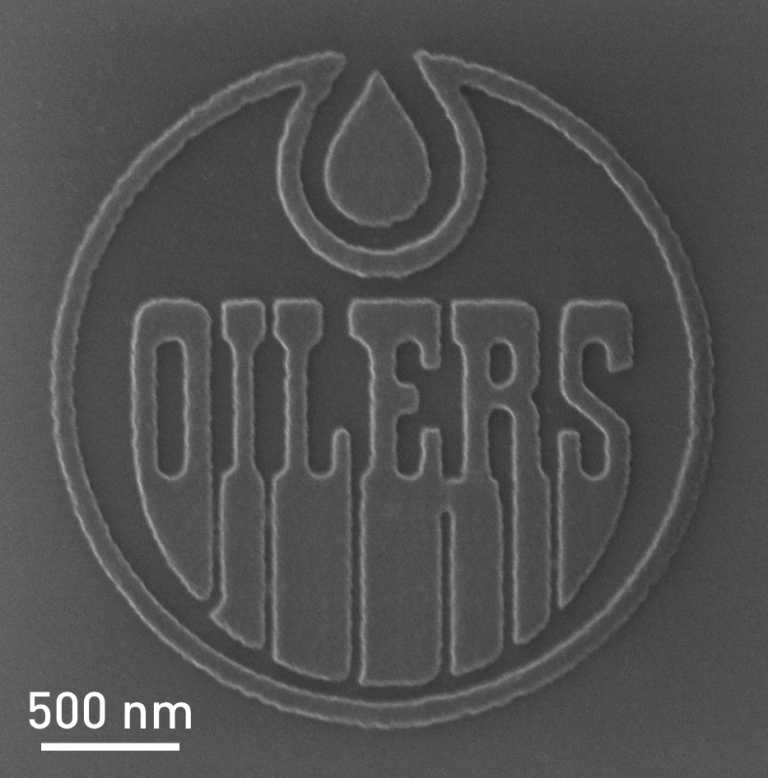
I have two news bits about Alberta’s nanotechnology scene, one focused on a hockey logo (this year [2017], there are two Canadian teams [Edmonton Oilers and Ottawa Senators] competing to get to the finals and a Stanley Cup win sometime in June; there hasn’t been a win by a Canadian team since 1993); the other news bit concerns funding for research into technology for oil spill cleanups.
National Hockey League (NHL) logo
To celebrate the Edmonton Oilers entry into the semifinals, folks at the University of Alberta have created the smallest NHL logo for them. From a May 1, 2017 news item by Chad Mosleh for Metro News Edmonton,
A department at the University of Alberta has created an Oilers logo so small you could fit 900 million of them on top of a puck.
“We’re constantly trying to push the limit of how small we can make things,” said Eric Flaim, director of the NanoFAB Fabrication & Characterization Centre, which focuses on research on micro and nanoscale units, which are particles so tiny you need an extremely powerful microscope to see them.
The microscopic Oilers logo was created in collaboration with Edmonton-based companies Applied Quantum Materials and Applied Nanotools. The logo is 2.4 micrometres in diameter, 40 times smaller than a similar one they made in 2006, which was roughly the width of a human hair. The university is calling it the world’s smallest NHL logo.
[downloaded from https://www.nanofab.ualberta.ca/2017/news/lets-go-oilers/]
An April 27, 2017 posting by Dr. Eric Flaim for the University of Alberta’s nanoFAB blog notes this (Note: Links have been removed),
Working in partnership with two Edmonton companies who are developing new nanoscale fabrication processes to support commercialization of made-in-Alberta technology for photonics, sensors, and nanomaterials, the nanoFAB took the opportunity to show pride in our Edmonton Oilers.
Using a nanomaterial developed by Applied Quantum Materials, and nanoscale pattern correction methods developed by Applied Nanotools, we thought it would be fitting to re-create the logo we fabricated during the Oilers’ last playoff run…albeit at a much smaller scale.
Whereas the Oilers logo in 2006 was about the width of a human hair, the logo we made for this year’s Orange Crush is over 40× smaller: at only 2.4 µm in diameter, over 900 million of these logos could fit on top of a hockey puck.
Beyond showing team spirit, the fabrication of this logo highlights several of the unique capabilities available at the nanoFAB. The logo was fabricated via electron-beam lithography (EBL) with our Raith 150-TWO system, using AQM SIOX as the EBL resist—a made-in-Edmonton alternative to the ultra-high resolution hydrogen silsesquioxane (HSQ) resist. At such a small length scale, sophisticated pattern correction techniques must be used to ensure the fidelity of the design; this expertise was provided by engineers from Applied Nanotools, who use the same methods for their high-resolution silicon photonics service. Finally, the images of the logos were taken using our Zeiss Orion NanoFab Helium Ion microscope.
I wonder how the University of Ottawa and the Ottawa Senators team are responding to this development?
Oil spills and carbon nanotube (CNT) meshes
An April 28, 2017 Ingenuity Lab news release (which rather weirdly has London, England listed as the location in the dateline) on MarketWired announces Canadian federal government funding for a project centered in Alberta, Canada,
Nanotechnology has had a multitude of applications: from healthcare to textiles to new consumer gadgets, innovative new uses for nanotechnology are constantly emerging. It has now found a new role, with University of Alberta-based nanotechnology accelerator Ingenuity Lab using it as the basis for the development of a revolutionary new way to clean up oil spills. The system has received a vote of confidence from Natural Resources Canada, with the organization providing $1.7m to fund its ongoing development.
Using a carbon-nanotube mesh combined with other minerals and polymers, Ingenuity Lab’s system acts as a sponge that attracts and absorbs oil underwater. When it is fully saturated with oil, the mesh is then removed from the water and exposed to heat, electricity or ultraviolet light, causing it to expel the collected oil.
The oil spill cleaning system has come a long way in a remarkably short amount of time. Director of Ingenuity Lab Dr Carlo Montemango [sic] said his team was able to demonstrate the effectiveness of the membrane approximately a year ago, but is now working on developing a large-scale version of the system. “Where you might see it is being rolled off the back [of a vessel] and dragged or moved through the water. As it becomes saturated, it would be brought on board, the oil would be expelled and it would be redeployed.”
Past tests have shown the system can be remarkably effective and is capable of cleaning up 100 percent of a spill – even the heavier oil that may be trapped below the surface. The system also recovers the oil, allowing it to be reused and potentially recuperate some of the cost associated with cleaning up a spill.
The technology is far more advanced than current methods of containing a spill, which usually involve floating booms and skimming oil from the water’s surface. Ingenuity Lab’s system would make a substantial difference should the world see another event on the scale of the 2010 Deepwater Horizon disaster, or the Exxon Valdez spill of 1989.
Montemango [sic] said the team is now working on developing a pilot system and beginning field tests in less than two years. “Our mission is to develop solutions to significant societal problems and challenges, and translate those solutions to the marketplace.”
I searched for more information about the new funding and found this news release (?) on the Ingenuity Lab website,
Oil is a common pollutant in oceans; more than three million metric tons of oil contaminate them every year. The accidental release of crude oil into a body of water by an oil tanker, refinery, storage facility, underwater pipeline, or offshore oil-drilling rig, is an environmental emergency. Depending on location, oil spills can be both hazardous as well as environmentally destructive. Timely cleanup is critical to protecting the integrity of the water, the shoreline, and the creatures that depend on these habitats. Due to increased scrutiny of the oil industry (with regards to its environmental record) the attention has focused on the development of new materials and technologies for removing organic contaminants; including spilled oil from waterways. Since existing methods are not sufficiently robust, nanotechnology has initiated the development of new tools using specifically designed materials suited for separations, such as the removal of crude oil from water.
Ingenuity Lab, a multidisciplinary research initiative based in Alberta, received $1.7 million in project funding for the research and development of an effective alternative for recovering heavy oil spilled in marine environments. IngenuityLab developed nanowire-based multifunctional stimuli-responsive membranes and devices capable of recovering the oil from spills.
This project will focus on the recovery of oil through the development of novel technology and devices using a variety of stimuli-responsive nanomaterials. The fabrication of reinforced membranes for oil-water separation (published in Adv. Mater. Interfaces, 2016, 3: 1600445) [emphasis mine] uses carbon nanotubes (CNTs), mats, and a few other metal oxide embedded nanowire hybrid membranes. They exhibit the switchable hydrophobic property with the influence of stimuli (UV, heat, electric, etc.). The focus of using the membranes is to develop a pilot facility for separating the oil out of spills to clean the environment while recovering the valuable oils.
Here’s a link to and a citation for the paper I highlighted in the news release (?),
I have a few comments about this work. it’s encouraging to see these efforts to develop better technologies for cleaning up oil spills but it does seem that none of these proposed solutions ever makes it out of the laboratory. For example, I have an April 17, 2012 posting about CNT nanosponges that absorb oil and which could be wrung out and reused. More recently, I had a Dec. 7, 2015 posting featuring boron nitride nanosponges (or nanosheets) for oil spill cleanups. Personally, I prefer sponges that can be wrung out over meshes or sponges that need additional processing such as exposure ” … to heat, electricity or ultraviolet light … .” Regardless, I hope one of these days, a new oil spill cleanup technology will make its way into the field.
For those not familiar with Alberta and the oil industry, the province is a main source for the fossil fuel and, in particular, the Alberta oil sands, which environmentalists have uncategorically condemned.
This research may help to commercialize use of carbon nanotubes (CNTs), a ‘magical’ nanoscale material with great promise and great difficulties (standardizing production being one of the main difficulties). A Feb. 10, 2017 news item on phys.org describes how researchers at the Lawrence Livermore National Laboratory (LLNL) and other collaborators have recorded carbon nanotubes self-organizing,
For the first time, Lawrence Livermore National Laboratory scientists and collaborators have captured a movie of how large populations of carbon nanotubes grow and align themselves.
Understanding how carbon nanotubes (CNT) nucleate, grow and self-organize to form macroscale materials is critical for application-oriented design of next-generation supercapacitors, electronic interconnects, separation membranes and advanced yarns and fabrics.
A Feb. 9, 2017 LLNL news release, which originated the news item, provides more information about the research (Note: Links have been removed),
New research by LLNL scientist Eric Meshot and colleagues from Brookhaven National Laboratory (link is external) (BNL) and Massachusetts Institute of Technology (link is external) (MIT) has demonstrated direct visualization of collective nucleation and self-organization of aligned carbon nanotube films inside of an environmental transmission electron microscope (ETEM).
In a pair of studies reported in recent issues of Chemistry of Materials (link is external) and ACS Nano (link is external), the researchers leveraged a state-of-the-art kilohertz camera in an aberration-correction ETEM at BNL to capture the inherently rapid processes that govern the growth of these exciting nanostructures.
Among other phenomena discovered, the researchers are the first to provide direct proof of how mechanical competition among neighboring carbon nanotubes can simultaneously promote self-alignment while also frustrating and limiting growth.
“This knowledge may enable new pathways toward mitigating self-termination and promoting growth of ultra-dense and aligned carbon nanotube materials, which would directly impact several application spaces, some of which are being pursued here at the Laboratory,” Meshot said.
Meshot has led the CNT synthesis development at LLNL for several projects, including those supported by the Laboratory Directed Research and Development (LDRD) program and the Defense Threat Reduction Agency (link is external) (DTRA) that use CNTs as fluidic nanochannels for applications ranging from single-molecule detection to macroscale membranes for breathable and protective garments.
Here’s a link to and a citation for the both of the papers mentioned in the news release,
The researchers have also provided this image which allows you to appreciate the difference between a ‘scientific’ version of the work and an artistic version,
This transmission electron microscope image shows growth of a dense carbon nanotube population. Courtesy: LLNL