Monthly Archives: July 2019

World’s smallest magnetic resonance imaging (MRI) of a single atom

While not science’s sleekest machine, this microscope was able to capture M.R.I. scans of single atoms. Credit: IBM Research

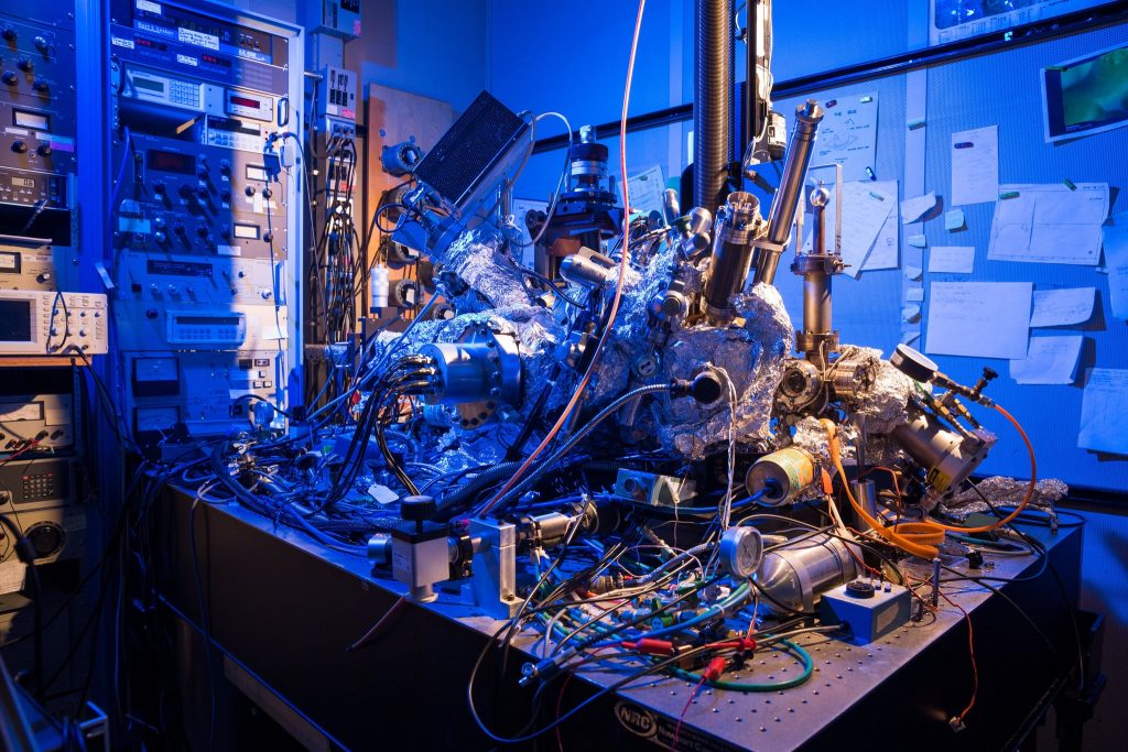
Such a messy looking thing—it makes me feel better about my housekeeping. In any event, it’s fascinating to think this scanning tunneling microscope as seen in the above can actually act as an MRI device and create an image of a single atom.

There’s a wonderful article in the New York Times about the work but I’m starting first with a July 1, 2019 news item on Nanowerk,

Researchers at the Center for Quantum Nanoscience (QNS) within the Institute for Basic Science (IBS) at Ewha Womans University [Seoul, South Korea) have made a major scientific breakthrough by performing the world’s smallest magnetic resonance imaging (MRI). In an international collaboration with colleagues from the US, QNS scientists used their new technique to visualize the magnetic field of single atoms.

A July 2, 2019 IBS news release (also on EurekAlert but published July 1, 2019), which originated the news item, provides some insight into the research,

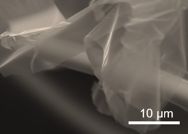
An MRI is routinely done in hospitals nowadays as a part of imaging for diagnostics. MRI’s detect the density of spins – the fundamental magnets in electrons and protons – in the human body. Traditionally, billions and billions of spins are required for an MRI scan. The new findings, published today [July 1, 2019] in the journal Nature Physics, show that this process is now also possible for an individual atom on a surface. To do this, the team used a Scanning Tunneling Microscope, which consists of an atomically sharp metal tip that allows researchers to image and probe single atoms by scanning the tip across the surface.

The two elements that were investigated in this work, iron and titanium, are both magnetic. Through precise preparation of the sample, the atoms were readily visible in the microscope. The researchers then used the microscope’s tip like an MRI machine to map the three-dimensional magnetic field created by the atoms with unprecedented resolution. In order to do so, they attached another spin cluster to the sharp metal tip of their microscope. Similar to everyday magnets, the two spins would attract or repel each other depending on their relative position. By sweeping the tip spin cluster over the atom on the surface, the researchers were able to map out the magnetic interaction. Lead author, Dr. Philip Willke of QNS says: “It turns out that the magnetic interaction we measured depends on the properties of both spins, the one on the tip and the one on the sample. For example, the signal that we see for iron atoms is vastly different from that for titanium atoms. This allows us to distinguish different kinds of atoms by their magnetic field signature and makes our technique very powerful.”

The researchers plan to use their single-atom MRI to map the spin distribution in more complex structures such as molecules and magnetic materials. “Many magnetic phenomena take place on the nanoscale, including the recent generation of magnetic storage devices.” says Dr. Yujeong Bae also of QNS, a co-author in this study. “We now plan to study a variety of systems using our microscopic MRI.” The ability to analyze the magnetic structure on the nanoscale can help to develop new materials and drugs. Moreover, the research team wants to use this kind of MRI to characterize and control quantum systems. These are of great interest for future computation schemes, also known as quantum computing

“I am very excited about these results. It is certainly a milestone in our field and has very promising implications for future research.” says Prof. Andreas Heinrich, Director of QNS. “The ability to map spins and their magnetic field with previously unimaginable precision, allows us to gain deeper knowledge about the structure of matter and opens new fields of basic research.”

The Center for Quantum Nanoscience, on the campus of Ewha Womans University in Seoul, South Korea, is a world-leading research center merging quantum and nanoscience to engineer the quantum future through basic research. Backed by Korea’s Institute for Basic Science, which was founded in 2011, the Center for Quantum Nanoscience draws on decades of QNS Director Andreas J. Heinrich’s (A Boy and His Atom, IBM, 2013) scientific leadership to lay the foundation for future technology by exploring the use of quantum behavior atom-by-atom on surfaces with highest precision.

You may have noticed that other than a brief mention in the first paragraph (in the Nanowerk news item excerpt), there’s no mention of the US researchers and their contribution to the work.

Interestingly, the July 1, 2019 New York Time article by Knvul Sheikh returns the favour by focusing almost entirely on US researchers while giving the Korean researchers a passing mention (Note: Links have been removed),

Different microscopy techniques allow scientists to see the nucleotide-by-nucleotide genetic sequences in cells down to the resolution of a couple atoms as seen in an atomic force microscopy image. But scientists at the IBM Almaden Research Center in San Jose, Calif., and the Institute for Basic Sciences in Seoul, have taken imaging a step further, developing a new magnetic resonance imaging technique that provides unprecedented detail, right down to the individual atoms of a sample.

When doctors want to detect tumors, measure brain function or visualize the structure of joints, they employ huge M.R.I. machines, which apply a magnetic field across the human body. This temporarily disrupts the protons spinning in the nucleus of every atom in every cell. A subsequent, brief pulse of radio-frequency energy causes the protons to spin perpendicular to the pulse. Afterward, the protons return to their normal state, releasing energy that can be measured by sensors and made into an image.

But to gather enough diagnostic data, traditional hospital M.R.I.s must scan billions and billions of protons in a person’s body, said Christopher Lutz, a physicist at IBM. So he and his colleagues decided to pack the power of an M.R.I. machine into the tip of another specialized instrument known as a scanning tunneling microscope to see if they could image individual atoms.

The tip of a scanning tunneling microscope is just a few atoms wide. And it moves along the surface of a sample, it picks up details about the size and conformation of molecules.

The researchers attached magnetized iron atoms to the tip, effectively combining scanning-tunneling microscope and M.R.I. technologies.

When the magnetized tip swept over a metal wafer of iron and titanium, it applied a magnetic field to the sample, disrupting the electrons (rather than the protons, as a typical M.R.I. would) within each atom. Then the researchers quickly turned a radio-frequency pulse on and off, so that the electrons would emit energy that could be visualized. …

Here’s a link to and a citation for the paper,

Magnetic resonance imaging of single atoms on a surface by Philip Willke, Kai Yang, Yujeong Bae, Andreas J. Heinrich & Christopher P. Lutz. Nature Physics (2019) DOI: https://doi.org/10.1038/s41567-019-0573-x Published 01 July 2019

This paper is behind a paywall.

Better performing solar cells with newly discovered property of pristine graphene

Light-harvesting devices—I like that better than solar cells or the like but I think that the term serves as a category rather than a name/label for a specific device. Enough musing. A December 17, 2018 news item on Nanowerk describes the latest about graphene and light-harvesting devices (Note: A link has been removed,

An international research team, co-led by a physicist at the University of California, Riverside, has discovered a new mechanism for ultra-efficient charge and energy flow in graphene, opening up opportunities for developing new types of light-harvesting devices.

The researchers fabricated pristine graphene — graphene with no impurities — into different geometric shapes, connecting narrow ribbons and crosses to wide open rectangular regions. They found that when light illuminated constricted areas, such as the region where a narrow ribbon connected two wide regions, they detected a large light-induced current, or photocurrent.

The finding that pristine graphene can very efficiently convert light into electricity could lead to the development of efficient and ultrafast photodetectors — and potentially more efficient solar panels.

A December 14, 2018 University of California at Riverside (UCR) news release by Iqbal Pittalwala (also on EurekAlert but published Dec. 17, 2018), which originated the news item,gives a brief description of graphene while adding context for this research,


Graphene, a 1-atom thick sheet of carbon atoms arranged in a hexagonal lattice, has many desirable material properties, such as high current-carrying capacity and thermal conductivity. In principle, graphene can absorb light at any frequency, making it ideal material for infrared and other types of photodetection, with wide applications in bio-sensing, imaging, and night vision.

In most solar energy harvesting devices, a photocurrent arises only in the presence of a junction between two dissimilar materials, such as “p-n” junctions, the boundary between two types of semiconductor materials. The electrical current is generated in the junction region and moves through the distinct regions of the two materials.

“But in graphene, everything changes,” said Nathaniel Gabor, an associate professor of physics at UCR, who co-led the research project. “We found that photocurrents may arise in pristine graphene under a special condition in which the entire sheet of graphene is completely free of excess electronic charge. Generating the photocurrent requires no special junctions and can instead be controlled, surprisingly, by simply cutting and shaping the graphene sheet into unusual configurations, from ladder-like linear arrays of contacts, to narrowly constricted rectangles, to tapered and terraced edges.”

Pristine graphene is completely charge neutral, meaning there is no excess electronic charge in the material. When wired into a device, however, an electronic charge can be introduced by applying a voltage to a nearby metal. This voltage can induce positive charge, negative charge, or perfectly balance negative and positive charges so the graphene sheet is perfectly charge neutral.

“The light-harvesting device we fabricated is only as thick as a single atom,” Gabor said. “We could use it to engineer devices that are semi-transparent. These could be embedded in unusual environments, such as windows, or they could be combined with other more conventional light-harvesting devices to harvest excess energy that is usually not absorbed. Depending on how the edges are cut to shape, the device can give extraordinarily different signals.”

The research team reports this first observation of an entirely new physical mechanism — a photocurrent generated in charge-neutral graphene with no need for p-n junctions — in Nature Nanotechnology today [Dec. 17, 2018].

Previous work by the Gabor lab showed a photocurrent in graphene results from highly excited “hot” charge carriers. When light hits graphene, high-energy electrons relax to form a population of many relatively cooler electrons, Gabor explained, which are subsequently collected as current. Even though graphene is not a semiconductor, this light-induced hot electron population can be used to generate very large currents.

“All of this behavior is due to graphene’s unique electronic structure,” he said. “In this ‘wonder material,’ light energy is efficiently converted into electronic energy, which can subsequently be transported within the material over remarkably long distances.”

He explained that, about a decade ago, pristine graphene was predicted to exhibit very unusual electronic behavior: electrons should behave like a liquid, allowing energy to be transferred through the electronic medium rather than by moving charges around physically.
“But despite this prediction, no photocurrent measurements had been done on pristine graphene devices — until now,” he said.

The new work on pristine graphene shows electronic energy travels great distances in the absence of excess electronic charge.

The research team has found evidence that the new mechanism results in a greatly enhanced photoresponse in the infrared regime with an ultrafast operation speed.
“We plan to further study this effect in a broad range of infrared and other frequencies, and measure its response speed,” said first author Qiong Ma, a postdoctoral associate in physics at the Massachusetts Institute of Technology, or MIT.

The researchers have provided an image illustrating their work,

Caption: Shining light on graphene: Although graphene has been studied vigorously for more than a decade, new measurements on high-performance graphene devices have revealed yet another unusual property. In ultra-clean graphene sheets, energy can flow over great distances, giving rise to an unprecedented response to light. Credit: Max Grossnickle and QMO Labs, UC Riverside.

Here’s a link to and a citation for the paper,

Giant intrinsic photoresponse in pristine graphene by Qiong Ma, Chun Hung Lui, Justin C. W. Song, Yuxuan Lin, Jian Feng Kong, Yuan Cao, Thao H. Dinh, Nityan L. Nair, Wenjing Fang, Kenji Watanabe, Takashi Taniguchi, Su-Yang Xu, Jing Kong, Tomás Palacios, Nuh Gedik, Nathaniel M. Gabor, & Pablo Jarillo-Herrero. Nature Nanotechnology (2018) Published 17 December 2018 DOI: https://doi.org/10.1038/s41565-018-0323-8

This paper is behind a paywall.

An artificial synapse tuned by light, a ferromagnetic memristor, and a transparent, flexible artificial synapse

Down the memristor rabbit hole one more time.* I started out with news about two new papers and inadvertently found two more. In a bid to keep this posting to a manageable size, I’m stopping at four.

UK

In a June 19, 2019 Nanowerk Spotlight article, Dr. Neil Kemp discusses memristors and some of his latest work (Note: A link has been removed),

Memristor (or memory resistors) devices are non-volatile electronic memory devices that were first theorized by Leon Chua in the 1970’s. However, it was some thirty years later that the first practical device was fabricated. This was in 2008 when a group led by Stanley Williams at HP Research Labs realized that switching of the resistance between a conducting and less conducting state in metal-oxide thin-film devices was showing Leon Chua’s memristor behaviour.

The high interest in memristor devices also stems from the fact that these devices emulate the memory and learning properties of biological synapses. i.e. the electrical resistance value of the device is dependent on the history of the current flowing through it.

There is a huge effort underway to use memristor devices in neuromorphic computing applications and it is now reasonable to imagine the development of a new generation of artificial intelligent devices with very low power consumption (non-volatile), ultra-fast performance and high-density integration.

These discoveries come at an important juncture in microelectronics, since there is increasing disparity between computational needs of Big Data, Artificial Intelligence (A.I.) and the Internet of Things (IoT), and the capabilities of existing computers. The increases in speed, efficiency and performance of computer technology cannot continue in the same manner as it has done since the 1960s.

To date, most memristor research has focussed on the electronic switching properties of the device. However, for many applications it is useful to have an additional handle (or degree of freedom) on the device to control its resistive state. For example memory and processing in the brain also involves numerous chemical and bio-chemical reactions that control the brain structure and its evolution through development.

To emulate this in a simple solid-state system composed of just switches alone is not possible. In our research, we are interested in using light to mediate this essential control.

We have demonstrated that light can be used to make short and long-term memory and we have shown how light can modulate a special type of learning, called spike timing dependent plasticity (STDP). STDP involves two neuronal spikes incident across a synapse at the same time. Depending on the relative timing of the spikes and their overlap across the synaptic cleft, the connection strength is other strengthened or weakened.

In our earlier work, we were only able to achieve to small switching effects in memristors using light. In our latest work (Advanced Electronic Materials, “Percolation Threshold Enables Optical Resistive-Memory Switching and Light-Tuneable Synaptic Learning in Segregated Nanocomposites”), we take advantage of a percolating-like nanoparticle morphology to vastly increase the magnitude of the switching between electronic resistance states when light is incident on the device.

We have used an inhomogeneous percolating network consisting of metallic nanoparticles distributed in filamentary-like conduction paths. Electronic conduction and the resistance of the device is very sensitive to any disruption of the conduction path(s).

By embedding the nanoparticles in a polymer that can expand or contract with light the conduction pathways are broken or re-connected causing very large changes in the electrical resistance and memristance of the device.

Our devices could lead to the development of new memristor-based artificial intelligence systems that are adaptive and reconfigurable using a combination of optical and electronic signalling. Furthermore, they have the potential for the development of very fast optical cameras for artificial intelligence recognition systems.

Our work provides a nice proof-of-concept but the materials used means the optical switching is slow. The materials are also not well suited to industry fabrication. In our on-going work we are addressing these switching speed issues whilst also focussing on industry compatible materials.

Currently we are working on a new type of optical memristor device that should give us orders of magnitude improvement in the optical switching speeds whilst also retaining a large difference between the resistance on and off states. We hope to be able to achieve nanosecond switching speeds. The materials used are also compatible with industry standard methods of fabrication.

The new devices should also have applications in optical communications, interfacing and photonic computing. We are currently looking for commercial investors to help fund the research on these devices so that we can bring the device specifications to a level of commercial interest.

If you’re interested in memristors, Kemp’s article is well written and quite informative for nonexperts, assuming of course you can tolerate not understanding everything perfectly.

Here are links and citations for two papers. The first is the latest referred to in the article, a May 2019 paper and the second is a paper appearing in July 2019.

Percolation Threshold Enables Optical Resistive‐Memory Switching and Light‐Tuneable Synaptic Learning in Segregated Nanocomposites by Ayoub H. Jaafar, Mary O’Neill, Stephen M. Kelly, Emanuele Verrelli, Neil T. Kemp. Advanced Electronic Materials DOI: https://doi.org/10.1002/aelm.201900197 First published: 28 May 2019

Wavelength dependent light tunable resistive switching graphene oxide nonvolatile memory devices by Ayoub H.Jaafar, N.T.Kemp. DOI: https://doi.org/10.1016/j.carbon.2019.07.007 Carbon Available online 3 July 2019

The first paper (May 2019) is definitely behind a paywall and the second paper (July 2019) appears to be behind a paywall.

Dr. Kemp’s work has been featured here previously in a January 3, 2018 posting in the subsection titled, Shining a light on the memristor.

China

This work from China was announced in a June 20, 2019 news item on Nanowerk,

Memristors, demonstrated by solid-state devices with continuously tunable resistance, have emerged as a new paradigm for self-adaptive networks that require synapse-like functions. Spin-based memristors offer advantages over other types of memristors because of their significant endurance and high energy effciency.

However, it remains a challenge to build dense and functional spintronic memristors with structures and materials that are compatible with existing ferromagnetic devices. Ta/CoFeB/MgO heterostructures are commonly used in interfacial PMA-based [perpendicular magnetic anisotropy] magnetic tunnel junctions, which exhibit large tunnel magnetoresistance and are implemented in commercial MRAM [magnetic random access memory] products.

“To achieve the memristive function, DW is driven back and forth in a continuous manner in the CoFeB layer by applying in-plane positive or negative current pulses along the Ta layer, utilizing SOT that the current exerts on the CoFeB magnetization,” said Shuai Zhang, a coauthor in the paper. “Slowly propagating domain wall generates a creep in the detection area of the device, which yields a broad range of intermediate resistive states in the AHE [anomalous Hall effect] measurements. Consequently, AHE resistance is modulated in an analog manner, being controlled by the pulsed current characteristics including amplitude, duration, and repetition number.”

“For a follow-up study, we are working on more neuromorphic operations, such as spike-timing-dependent plasticity and paired pulsed facilitation,” concludes You. …

Here’s are links to and citations for the paper (Note: It’s a little confusing but I believe that one of the links will take you to the online version, as for the ‘open access’ link, keep reading),

A Spin–Orbit‐Torque Memristive Device by Shuai Zhang, Shijiang Luo, Nuo Xu, Qiming Zou, Min Song, Jijun Yun, Qiang Luo, Zhe Guo, Ruofan Li, Weicheng Tian, Xin Li, Hengan Zhou, Huiming Chen, Yue Zhang, Xiaofei Yang, Wanjun Jiang, Ka Shen, Jeongmin Hong, Zhe Yuan, Li Xi, Ke Xia, Sayeef Salahuddin, Bernard Dieny, Long You. Advanced Electronic Materials Volume 5, Issue 4 April 2019 (print version) 1800782 DOI: https://doi.org/10.1002/aelm.201800782 First published [online]: 30 January 2019 Note: there is another DOI, https://doi.org/10.1002/aelm.201970022 where you can have open access to Memristors: A Spin–Orbit‐Torque Memristive Device (Adv. Electron. Mater. 4/2019)

The paper published online in January 2019 is behind a paywall and the paper (almost the same title) published in April 2019 has a new DOI and is open access. Final note: I tried accessing the ‘free’ paper and opened up a free file for the artwork featuring the work from China on the back cover of the April 2019 of Advanced Electronic Materials.

Korea

Usually when I see the words transparency and flexibility, I expect to see graphene is one of the materials. That’s not the case for this paper (link to and citation for),

Transparent and flexible photonic artificial synapse with piezo-phototronic modulator: Versatile memory capability and higher order learning algorithm by Mohit Kumar, Joondong Kim, Ching-Ping Wong. Nano Energy Volume 63, September 2019, 103843 DOI: https://doi.org/10.1016/j.nanoen.2019.06.039 Available online 22 June 2019

Here’s the abstract for the paper where you’ll see that the material is made up of zinc oxide silver nanowires,

An artificial photonic synapse having tunable manifold synaptic response can be an essential step forward for the advancement of novel neuromorphic computing. In this work, we reported the development of highly transparent and flexible two-terminal ZnO/Ag-nanowires/PET photonic artificial synapse [emphasis mine]. The device shows purely photo-triggered all essential synaptic functions such as transition from short-to long-term plasticity, paired-pulse facilitation, and spike-timing-dependent plasticity, including in the versatile memory capability. Importantly, strain-induced piezo-phototronic effect within ZnO provides an additional degree of regulation to modulate all of the synaptic functions in multi-levels. The observed effect is quantitatively explained as a dynamic of photo-induced electron-hole trapping/detraining via the defect states such as oxygen vacancies. We revealed that the synaptic functions can be consolidated and converted by applied strain, which is not previously applied any of the reported synaptic devices. This study will open a new avenue to the scientific community to control and design highly transparent wearable neuromorphic computing.

This paper is behind a paywall.

Jiggly jell-o as a new hydrogen fuel catalyst

Jello [uploaded from https://www.organicauthority.com/eco-chic-table/new-jell-o-mold-jiggle-chic-holidays]

I’m quite intrigued by this ‘jell-o’ story. It’s hard to believe a childhood dessert might prove to have an application as a catalyst for producing hydrogen fuel. From a December 14, 2018 news item on Nanowerk,

A cheap and effective new catalyst developed by researchers at the University of California, Berkeley, can generate hydrogen fuel from water just as efficiently as platinum, currently the best — but also most expensive — water-splitting catalyst out there.

The catalyst, which is composed of nanometer-thin sheets of metal carbide, is manufactured using a self-assembly process that relies on a surprising ingredient: gelatin, the material that gives Jell-O its jiggle.

Two-dimensional metal carbides spark a reaction that splits water into oxygen and valuable hydrogen gas. Berkeley researchers have discovered an easy new recipe for cooking up these nanometer-thin sheets that is nearly as simple as making Jell-O from a box. (Xining Zang graphic, copyright Wiley)

A December 13, 2018 University of California at Berkeley (UC Berkeley) news release by Kara Manke (also on EurekAlert but published on Dec. 14, 2018), which originated the news item, provides more technical detail,

“Platinum is expensive, so it would be desirable to find other alternative materials to replace it,” said senior author Liwei Lin, professor of mechanical engineering at UC Berkeley. “We are actually using something similar to the Jell-O that you can eat as the foundation, and mixing it with some of the abundant earth elements to create an inexpensive new material for important catalytic reactions.”

The work appears in the Dec. 13 [2018] print edition of the journal Advanced Materials.

A zap of electricity can break apart the strong bonds that tie water molecules together, creating oxygen and hydrogen gas, the latter of which is an extremely valuable source of energy for powering hydrogen fuel cells. Hydrogen gas can also be used to help store energy from renewable yet intermittent energy sources like solar and wind power, which produce excess electricity when the sun shines or when the wind blows, but which go dormant on rainy or calm days.

A black and white image of metal carbide under high magnification.

When magnified, the two-dimensional metal carbides resemble sheets of cell[o]phane. (Xining Zang photo, copyright Wiley)

But simply sticking an electrode in a glass of water is an extremely inefficient method of generating hydrogen gas. For the past 20 years, scientists have been searching for catalysts that can speed up this reaction, making it practical for large-scale use.

“The traditional way of using water gas to generate hydrogen still dominates in industry. However, this method produces carbon dioxide as byproduct,” said first author Xining Zang, who conducted the research as a graduate student in mechanical engineering at UC Berkeley. “Electrocatalytic hydrogen generation is growing in the past decade, following the global demand to lower emissions. Developing a highly efficient and low-cost catalyst for electrohydrolysis will bring profound technical, economical and societal benefit.”

To create the catalyst, the researchers followed a recipe nearly as simple as making Jell-O from a box. They mixed gelatin and a metal ion — either molybdenum, tungsten or cobalt — with water, and then let the mixture dry.

“We believe that as gelatin dries, it self-assembles layer by layer,” Lin said. “The metal ion is carried by the gelatin, so when the gelatin self-assembles, your metal ion is also arranged into these flat layers, and these flat sheets are what give Jell-O its characteristic mirror-like surface.”

Heating the mixture to 600 degrees Celsius triggers the metal ion to react with the carbon atoms in the gelatin, forming large, nanometer-thin sheets of metal carbide. The unreacted gelatin burns away.

The researchers tested the efficiency of the catalysts by placing them in water and running an electric current through them. When stacked up against each other, molybdenum carbide split water the most efficiently, followed by tungsten carbide and then cobalt carbide, which didn’t form thin layers as well as the other two. Mixing molybdenum ions with a small amount of cobalt boosted the performance even more.

“It is possible that other forms of carbide may provide even better performance,” Lin said.

On the left, an illustration of blue spheres, representing gelatin molecules, arranged in a lattice shape. On the right, an illustration of thin sheets of metal carbide.

Molecules in gelatin naturally self-assemble in flat sheets, carrying the metal ions with them (left). Heating the mixture to 600 degrees Celsius burns off the gelatin, leaving nanometer-thin sheets of metal carbide. (Xining Zang illustration, copyright Wiley)

The two-dimensional shape of the catalyst is one of the reasons why it is so successful. That is because the water has to be in contact with the surface of the catalyst in order to do its job, and the large surface area of the sheets mean that the metal carbides are extremely efficient for their weight.

Because the recipe is so simple, it could easily be scaled up to produce large quantities of the catalyst, the researchers say.

“We found that the performance is very close to the best catalyst made of platinum and carbon, which is the gold standard in this area,” Lin said. “This means that we can replace the very expensive platinum with our material, which is made in a very scalable manufacturing process.”

Co-authors on the study are Lujie Yang, Buxuan Li and Minsong Wei of UC Berkeley, J. Nathan Hohman and Chenhui Zhu of Lawrence Berkeley National Lab; Wenshu Chen and Jiajun Gu of Shanghai Jiao Tong University; Xiaolong Zou and Jiaming Liang of the Shenzhen Institute; and Mohan Sanghasadasa of the U.S. Army RDECOM AMRDEC.

Here’s a link to and a citation for the paper,

Self‐Assembly of Large‐Area 2D Polycrystalline Transition Metal Carbides for Hydrogen Electrocatalysis by Xining Zang, Wenshu Chen, Xiaolong Zou, J. Nathan Hohman, Lujie Yang
Buxuan Li, Minsong Wei, Chenhui Zhu, Jiaming Liang, Mohan Sanghadasa, Jiajun Gu, Liwei Lin. Advanced Materials Volume30, Issue 50 December 13, 2018 1805188 DOI: https://doi.org/10.1002/adma.201805188 First published [online]: 09 October 2018

This paper is behind a paywall.

Science events and an exhibition concerning wind in the Vancouver (Canada) area for July 2019 and beyond

it’s not quite the bumper crop of science events that took place in May 2019, which may be a good thing if you’re eager to attend everything. First, here are the events and then, the exhibition.

Nerd Nite at the Movies

On July 10, 2019, a new series is being launched at the Vancouver International Film Festival (VIFF) Centre. Here’s the description from the Nerd Nite Vancouver SciFact vs SciFi: Nerd Nite Goes to the Movies event page,

SciFact vs SciFiction: Nerd Nite Goes to the Movies v1. Animal

This summer we’re trying something a little different. Our new summer series of talks – a collaboration between Nerd Nite and VIFF – examines the pseudo-science propagated by Hollywood, and seeks to sift real insights from fake facts, in a fun, playful but peer-approved format. Each show will feature clips from a variety of movies on a science theme with a featured scientist on hand all done Nerd Nite style with drinks! We begin with biology, and our first presenter is Dr Carin Bondar.

Dr Bondar has been the host of Science Channel’s Outrageous Acts of Science, and she’s the author of several books including “Wild Moms: The Science Behind Mating in the Animal Kingdom”. Tonight she’ll join Kaylee [Byers] and Michael [Unger] from Nerd Nite to discuss the sci-facts in a variety of clips from cinema. We’ll be discussing the science in Planet of the ApesThe BirdsArachnophobiaSnakes on a Plane, and more!

When: July 10 [2019]
Where: Vancouver International Film Centre
When: 7:30 – 8:30 – This talk will be followed by a screening of Alfred Hitchcock’s classic The Birds (9pm). Double bill price: $20
Tickets: Here!

The VIFF Centre’s SciFact vs SciFi: Animals According to Hollywood event page has much the same information plus this,

SciFact vs SciFi: Nerd Nite Goes to the Movies continues:

July 31 [2019] – Dr. Douglas Scott: The Universe According to Hollywood
Aug 14 [2019] – Mika McKinnon: Disaster According to Hollywood
Aug 28 [2019] – Greg Bole: Evolution According to Hollywood

This series put me in mind what was then the New York-based, ‘Science Goes to the Movies’. I first mentioned this series in a March 10, 2016 posting and it seems that since then, the series has lost a host and been embraced by public television (in the US). You can find the latest incarnation of Science Goes To The Movies here.

Getting back to Vancouver, no word as to which movies will accompany these future talks. If I had a vote, I’d love to see Gattaca accompany any talk on genetics.

That last sentence is both true and provides a neat segue to the next event.

Genetics at the Vancouver Public Library (VPL)

Coming up on July 23, 2019, a couple of graduate students at the University of British Columbia will be sharing some of the latest information on genetics. From the VPL events page,

Curiosities of the Natural World: Genetics – the Future of Medicine

Tuesday, July 23, 2019 (7:00 pm – 8:30 pm)
Central Library
Description

Since their discovery over a century ago, diabetes, multiple sclerosis, and Alzheimer’s have seemed like diseases without a cure. The advent of genetic treatments and biomarkers are changing the outcomes and treatments of these once impossible-to-treat conditions.

UBC researchers, Adam Ramzy and Maria-Elizabeth Baeva discuss the potential of genetic therapies for diabetes, and new biomarkers and therapeutics for Alzheimer ’s disease and multiple sclerosis.

This program is part of the Curiosities of the Natural World series in partnership with UBC Let’s Talk Science, the UBC Faculty of Science, and the UBC Public Scholars Initiative

Suitable for: Adults
Seniors

Additional Details:
Alma VanDusen and Peter Kaye Rooms, Lower Level

It’s hard to know how to respond to this as I loathe anything that has ‘future of medicine’ in it. Isn’t there always going to ***be*** ‘a’ future with medicine in it?

Also, there is at least one cautionary tale about this new era of ‘genetic medicine’: Glybera is a gene therapy that worked for people with a rare genetic disease. It is a **treatment**, the only one, and it is no longer available.

Kelly Crowe in a November 17, 2018 article for the CBC (Canadian Broadcasting Corporation) news writes about Glybera,

It is one of this country’s great scientific achievements.

The first drug ever approved that can fix a faulty gene.

It’s called Glybera, and it can treat a painful and potentially deadly genetic disorder with a single dose — a genuine made-in-Canada medical breakthrough.

But most Canadians have never heard of it.

A team of researchers at the University of British Columbia spent decades developing the treatment for people born with a genetic mutation that causes lipoprotein lipase disorder (LPLD).

LPLD affects communities in the Saguenay region of northeastern Quebec at a higher rate than anywhere else in the world.

Glybera was never sold in North America and was available in Europe for just two years, beginning in 2015. During that time, only one patient received the drug. Then it was abandoned by the company that held its European licensing rights.

The problem was the price.

The world’s first gene therapy, a remarkable discovery by a dedicated team of scientists who came together in a Vancouver lab, had earned a second, more dubious distinction:

The world’s most expensive drug.

It cost $1M for a single treatment and that single treatment is good for at least 10 years.

Pharmaceutical companies make their money from repeated use of their medicaments and Glybera required only one treatment so the company priced it according to how much they would have gotten for repeated use, $100,000 per year over a 10 year period. The company was not able to persuade governments and/or individuals to pay the cost.

In the end, 31 people got the treatment, most of them received it for free through clinical trials.

Crowe has written an exceptionally good story (November 17, 2018 article) about Glybera and I encourage you to read in its entirety. I warn you it’s heartbreaking.

I wrote about money and genetics in an April 26, 2019 posting (Gene editing and personalized medicine: Canada). Scroll down to the subsection titled ‘Cost/benefit analysis’ for a mention of Goldman Sachs, an American global investment banking, securities and investment management firm, and its conclusion that personalized medicine is not a viable business model. I wonder if part of their analysis included the Glybera experience.

Getting back to the July 23, 2019 talk at the VPL’s central branch, I have no doubt the researchers will be discussing some exciting work but the future might not be as rosy as one might hope.

I wasn’t able to find much information about either Adan Ramzy or Maria-Elizabeth Baeva. There’s this for Ramzy (scroll down to Class of 2021) and this for Baeva (scroll down to Scholarships).

WINDS from June 22 to September 29, 2019

This show or exhibition is taking place in New Westminster (part of the Metro Vancouver area) at the Anvil Centre’s New Media Gallery. From the Anvil Centre’s WINDS event page,

WINDS
New Media Gallery Exhibition
June 22  – September 29
Opening Reception + Artist Talk  is on June 21st at 6:30pm
 
Chris Welsby (UK)
Spencer Finch (UK)
David Bowen (USA)
Nathalie Miebach (Germany/USA)
 
Our summer exhibition features four exciting, multi-media installations by four international artists from UK and USA.  Each artist connects with the representation, recreation and manifestation of wind through physical space and time.  Each suggests how our perception and understanding of wind can be created through pressure, sound, data, pattern, music and motion and then further appreciated in poetic or metaphoric ways that might connect us with how the wind influences language, imagination or our understanding of historic events.
 
All the artists use sound as a key element ; to emphasize or recreate the sonic experience of different winds and their effects, to trigger memory or emotion, or to heighten certain effects that might prompt the viewer to consider significant philosophical questions. Common objects are used in all the works; discarded objects, household or readymade objects and everyday materials; organic, synthetic, natural and manmade. The viewer will find connections with past winds and events both recent and distant.  There is an attempt to capture or allude to a moment in time which brings with it suggestions of mortality,  thereby transforming the works into poignant memento-mori.

Dates
June 22 – September 29, 2019

Price
Complimentary

Location
777 Columbia Street. New Media Gallery.

The New Media Gallery’s home page features ‘winds’ (yes, it’s all in lower case),

Landscape and weather have long shared an intimate connection with the arts.  Each of the works here is a landscape: captured, interpreted and presented through a range of technologies. The four artists in this exhibition have taken, as their material process, the movement of wind through physical space & time. They explore how our perception and understanding of landscape can be interpreted through technology. 

These works have been created by what might be understood as a sort of scientific method or process that involves collecting data, acute observation, controlled experiments and the incorporation of measurements and technologies that control or collect motion, pressure, sound, pattern and the like. The artists then take us in other directions; allowing technology or situations to render visible that which is invisible, creating and focussing on peculiar or resonant qualities of sound, light or movement in ways that seem to influence emotion or memory, dwelling on iconic places and events, or revealing in subtle ways, the subjective nature of time.  Each of these works suggest questions related to the nature of illusive experience and how or if it can be captured, bringing inevitable connections to authorship, loss, memory and memento mori

David Bowen
tele-present wind
Image
Biography
Credits

Spencer Finch (USA)
2 hours, 2 minutes, 2 seconds (Wind at Walden Pond, March 12, 2007)
Image
Biography
Credits

Nathalie Miebach (USA)
Hurricane Noel III
Image
Biography
Credits

Chris Welsby (UK)
Wind Vane
Image
Biography
Credits

Hours
10:00am – 5:00pm Tuesday – Sunday
10:00am – 8:00pm Thursdays
Closed Monday

Address
New Media Gallery
3rd Floor Anvil Centre
777 Columbia Street
New Westminster, BC V3M 1B6

If you want to see the images and biographies for the artists participating in ‘winds’, please go here..

So there you have it, science events and an exhibition in the Vancouver* area for July 2019.

*July 23, 2019 Correction: The word ‘and’ was removed from the final sentence for grammatical correctness.

**July 23, 2019 Correction: I changed the word ‘cure’ to ‘treatment’ so as to be more accurate. The word ‘cure’ suggests permanence and Glybera is supposed to be effective for 10 years or longer but no one really knows.

***Added the word ‘be’ for grammatical correctness on Nov. 30, 2020.

Better anti-parasitic medicine delivery with chitosan-based nanocapsules

I mage: The common liver fluke which can cause fascioliasis. Credit: Wikimedia creative commons Courtesy: Leeds University

It looks like a pair of lips to me but, according to a December 12, 2018 news item on Nanowerk, this liver fluke heralds a flatworm infection is a serious health problem,

An international team, led by Professor Francisco Goycoolea from the University of Leeds [UK] and Dr Claudio Salomon from the Universidad Nacional de Rosario, Argentina, and in collaboration with colleagues at the University of Münster, Germany, have developed a novel pharmaceutical formulation to administer triclabendazole – an anti-parasitic drug used to treat a type of flatworm infection – in billions of tiny capsules.

The World Health Organisation estimates that 2.4 million people are infected with fascioliasis, the disease caused by flatworms and treated with triclabendazole.

A December 12, 2018 University of Leeds  press release (also on EurekAlert), which originated the news item,

Anti-parasitic drugs do not become effective until they dissolve and are absorbed. Traditionally, these medicines are highly insoluble and this limits their therapeutic effect.
In a bid to overcome this limitation and accomplish the new formulation, the team used “soft” nanotechnology and nanomedicine approaches, which utilises the self-assembly properties of organic nanostructures and uses techniques in which components, such as polymers and surfactants in solution, play key roles.

Their formulation produces capsules that are less than one micron in size – the diameter of a human hair is roughly 75 microns. These tiny capsules are loaded with triclabendazole and then bundled together to deliver the required dose.

The team used chitosan, a naturally-occurring sugar polymer found in the exoskeleton of shellfish and the cell walls of certain fungi, to coat the oil-core of capsules and bind the drug together, while stabilising the capsule and helping to preserve it.
In its nanocapsule form, the drug would be 100 times more soluble than its current tablet form.

Professor Goycoolea, from the School of Food Science and Nutrition at Leeds, said: “Solubility is critical challenge for effective anti-parasite medicine. We looked to tackle this problem at the particle level. Triclabendazole taken as a dose made up of billions of tiny capsules would mean the medicine would be more efficiently and quickly absorbed

“Through the use of nanocapsules and nanoemulsions, drug efficiency can be enhanced and new solutions can be considered for the best ways to target medicine delivery.”
Dr Salomon said: “To date, this is the first report on triclabendazole nanoencapsulation and we believe this type of formulation could be applied to other anti-parasitic drugs as well. But more research is needed to ensure this new pharmaceutical formulation of the drug does not diminish the anti-parasitic effect. Our ongoing research is working to answer this very question.”

Although there have been cases of fascioliasis in more than 70 countries worldwide, with increasing reports from Europe and the Americas, it is considered a neglected disease, as it does not receive much attention and often goes untreated.
Symptoms of the disease when it reaches the chronic phase include intermittent pain, jaundice and anaemia. Patients can also experience hardening of the liver in the case of long-term inflammation.

Because of the highly insoluble nature of anti-parasitic drugs, they need to be administered in very high dosages to ensure enough of the active ingredient is absorbed. This is particularly problematic when treating children for parasites. Tablets needs to be divided into smaller pieces to adjust the dosage and make swallowing easier, but this can cause side effects due to incorrect dosage.

The team’s technique to formulate triclabendazole into nanocapsules, published today [Dec. 12, 2018] in the journal PLOS ONE, would also allow for lower doses to be administered. s

Here’s a link to and a citation for the paper,

Chitosan-based nanodelivery systems applied to the development of novel triclabendazole formulations by Daniel Real, Stefan Hoffmann, Darío Leonardi, Claudio Salomon, Francisco M. Goycoolea. PLOS DOI https://doi.org/10.1371/journal.pone.0207625 Published: December 12, 2018

This paper is open access. BTW, I loved the title for the press release (Helping the anti-parasitic medicine go down) for its reference to the song, A spoonful of sugar helps the medicine go down, in the 1964 film musical, Mary Poppins, and the shout out for the sort of sequel, Mary Poppins Returns, released on Dec. 19, 2018.

CARESSES your elders (robots for support)

Culturally sensitive robots for elder care! It’s about time. The European Union has funded the Culture Aware Robots and Environmental Sensor Systems for Elderly Support (CARESSES) project being coordinated in Italy. A December 13, 2018 news item on phys.org describes the project,

Researchers have developed revolutionary new robots that adapt to the culture and customs of the elderly people they assist.

Population ageing has implications for many sectors of society, one of which is the increased demand on a country’s health and social care resources. This burden could be greatly eased through advances in artificial intelligence. Robots have the potential to provide valuable assistance to caregivers in hospitals and care homes. They could also improve home care and help the elderly live more independently. But to do this, they will have to be able to respond to older people’s needs in a way that is more likely to be trusted and accepted.
The EU-funded project CARESSES has set out to build the first ever culturally competent robots to care for the elderly. The groundbreaking idea involved designing these robots to adapt their way of acting and speaking to match the culture and habits of the elderly person they’re assisting.

“The idea is that robots should be capable of adapting to human culture in a broad sense, defined by a person’s belonging to a particular ethnic group. At the same time, robots must be able to adapt to an individual’s personal preferences, so in that sense, it doesn’t matter if you’re Italian or Indian,” explained researcher Alessandro Saffiotti of project partner Örebro University, Sweden, …

A December 13, 2018 (?) CORDIS press release, which originated the news item, adds more detail about the robots and their anticipated relationship to their elderly patients,

Through its communication with an elderly person, the robot will fine-tune its knowledge by adapting it to that person’s cultural identity and individual characteristics. Using this knowledge, it will be able to remind the elderly person to take their prescribed medication, encourage them to eat healthily and be active, or help them stay in touch with family and friends. The robot will also be able to make suggestions about the appropriate clothing for specific occasions and remind people of upcoming religious and other celebrations. It doesn’t replace a care home worker. Nevertheless, it will play a vital role in helping to make elderly people’s lives less lonely and reducing the need to have a caregiver nearby at all times.

Scientists are testing the first CARESSES robots in care homes in the United Kingdom and Japan. They’re being used to assist elderly people from different cultural backgrounds. The aim is to see if people feel more comfortable with robots that interact with them in a culturally sensitive manner. They’re also examining whether such robots improve the elderly’s quality of life. “The testing of robots outside of the laboratory environment and in interaction with the elderly will without a doubt be the most interesting part of our project,” added Saffiotti.

The innovative CARESSES (Culture Aware Robots and Environmental Sensor Systems for Elderly Support) robots may pave the way to more culturally sensitive services beyond the sphere of elderly care, too. “It will add value to robots intended to interact with people. Which is not to say that today’s robots are completely culture-neutral. Instead, they unintentionally reflect the culture of the humans who build and program them.”

Having had a mother who recently died in a care facility, I can testify to the importance of cultural and religious sensitivity on the part of caregivers. As for this type of robot not replacing anyone, I take that with a grain of salt. They always say that and I expect it’s true in the initial stages but once the robots are well established and working well? Why not? After all, they’re cheaper in many, many ways and with the coming tsunami of elders in many countries around the world, it seems to me that displacement by robots is an inevitability.