Category Archives: light

Quantum processor woven from light

Weaving a quantum processor from light is a jaw-dropping event (as far as I’m concerned). An October 17, 2019 news item on phys.org makes the announcement,

An international team of scientists from Australia, Japan and the United States has produced a prototype of a large-scale quantum processor made of laser light.

Based on a design ten years in the making, the processor has built-in scalability that allows the number of quantum components—made out of light—to scale to extreme numbers. The research was published in Science today [October 18, 2019; Note: I cannot explain the discrepancy between the dates]].

Quantum computers promise fast solutions to hard problems, but to do this they require a large number of quantum components and must be relatively error free. Current quantum processors are still small and prone to errors. This new design provides an alternative solution, using light, to reach the scale required to eventually outperform classical computers on important problems.

Caption: The entanglement structure of a large-scale quantum processor made of light. Credit: Shota Yokoyama 2019

An October 18, 2019 RMIT University (Australia) press release (also on EurekAlert but published October 17, 2019), which originated the news time, expands on the theme,

“While today’s quantum processors are impressive, it isn’t clear if the current designs can be scaled up to extremely large sizes,” notes Dr Nicolas Menicucci, Chief Investigator at the Centre for Quantum Computation and Communication Technology (CQC2T) at RMIT University in Melbourne, Australia.

“Our approach starts with extreme scalability – built in from the very beginning – because the processor, called a cluster state, is made out of light.”

Using light as a quantum processor

A cluster state is a large collection of entangled quantum components that performs quantum computations when measured in a particular way.

“To be useful for real-world problems, a cluster state must be both large enough and have the right entanglement structure. In the two decades since they were proposed, all previous demonstrations of cluster states have failed on one or both of these counts,” says Dr Menicucci. “Ours is the first ever to succeed at both.”

To make the cluster state, specially designed crystals convert ordinary laser light into a type of quantum light called squeezed light, which is then weaved into a cluster state by a network of mirrors, beamsplitters and optical fibres.

The team’s design allows for a relatively small experiment to generate an immense two-dimensional cluster state with scalability built in. Although the levels of squeezing – a measure of quality – are currently too low for solving practical problems, the design is compatible with approaches to achieve state-of-the-art squeezing levels.

The team says their achievement opens up new possibilities for quantum computing with light.

“In this work, for the first time in any system, we have made a large-scale cluster state whose structure enables universal quantum computation.” Says Dr Hidehiro Yonezawa, Chief Investigator, CQC2T at UNSW Canberra. “Our experiment demonstrates that this design is feasible – and scalable.”

###

The experiment was an international effort, with the design developed through collaboration by Dr Menicucci at RMIT, Dr Rafael Alexander from the University of New Mexico and UNSW Canberra researchers Dr Hidehiro Yonezawa and Dr Shota Yokoyama. A team of experimentalists at the University of Tokyo, led by Professor Akira Furusawa, performed the ground-breaking experiment.

Here’s a link to and a citation for the paper,

Generation of time-domain-multiplexed two-dimensional cluster state by Warit Asavanant, Yu Shiozawa, Shota Yokoyama, Baramee Charoensombutamon, Hiroki Emura, Rafael N. Alexander, Shuntaro Takeda, Jun-ichi Yoshikawa, Nicolas C. Menicucci, Hidehiro Yonezawa, Akira Furusawa. Science 18 Oct 2019: Vol. 366, Issue 6463, pp. 373-376 DOI: 10.1126/science.aay2645

This paper is behind a paywall.

Colloidal quantum dots as ultra-sensitive hyper-spectral photodetectors

An October 16, 2019 news item on Nanowerk announces some of the latest work with colloidal quantum dots,

Researchers of the Optoelectronics and Measurement Techniques Unit (OPEM) at the University of Oulu [Finland] have invented a new method of producing ultra-sensitive hyper-spectral photodetectors. At the heart of the discovery are colloidal quantum dots, developed together with the researchers at the University of Toronto, Canada.

Quantum dots are tiny particles of 15-150 atoms of semiconducting material that have extraordinary optical and electrical properties due to quantum mechanics phenomena.

By controlling the size of the dots, the researchers are able to finetune how they react to different light colors (light wavelengths), especially those invisible for the human eye, namely the infrared spectrum.

The figure briefly introduces the concept of the study conducted by the researchers of the University of Oulu and the University of Toronto. The solution consisting of colloidal quantum dots is inkjet-printed, creating active photosensitive layer of the photodetector. Courtesy: Oulu University

An October 16, 2019 Oulu University press release, which originated the news item, provides more detail,

-Naturally, it is very rewarding that our hard work has been recognized by the international scientific community but at the same time, this report helps us to realize that there is a long journey ahead in incoming years. This publication is especially satisfying because it is the result of collaboration with world-class experts at the University of Toronto, Canada. This international collaboration where we combined the expertise of Toronto’s researchers in synthesizing quantum dots and our expertise in printed intelligence resulted in truly unique devices with astonishing performance, says docent Rafal Sliz, a leading researcher in this project.
 
Mastered in the OPEM unit, inkjet printing technology makes possible the creation of optoelectronic devices by designing functional inks that are printed on various surfaces, for instance, flexible substrates, clothing or human skin. Inkjet printing combined with colloidal quantum dots allowed the creation of photodetectors of impresive detectivity characteristics. The developed technology is a milestone in the creation of a new type of sub-micron-thick, flexible, and inexpensive IR sensing devices, the next generation of solar cells and other novel photonic systems.

-Oulus’ engineers and scientists’ strong expertise in optoelectronics resulted in many successful Oulu-based companies like Oura, Specim, Focalspec, Spectral Engines, and many more. New optoelectronic technologies, materials, and methods developed by our researchers will help Oulu and Finland to stay at the cutting edge of innovation, says professor Tapio Fabritius, a leader of the OPEM.

Here’s a link to and a citation for the paper,

Stable Colloidal Quantum Dot Inks Enable Inkjet-Printed High-Sensitivity Infrared Photodetectors by Rafal Sliz, Marc Lejay, James Z. Fan, Min-Jae Choi, Sachin Kinge, Sjoerd Hoogland, Tapio Fabritius, F. Pelayo García de Arquer, Edward H. Sargent. ACS Nano 2019 DOI: https://doi.org/10.1021/acsnano.9b06125 Publication Date:September 23, 2019 Copyright © 2019 American Chemical Society

This paper is behind a paywall.

Using light to manipulate neurons

There are three (or more?) possible applications including neuromorphic computing for this new optoelectronic technology which is based on black phophorus. A July 16, 2019 news item on Nanowerk announces the research,

Researchers from RMIT University [Australia] drew inspiration from an emerging tool in biotechnology – optogenetics – to develop a device that replicates the way the brain stores and loses information.

Optogenetics allows scientists to delve into the body’s electrical system with incredible precision, using light to manipulate neurons so that they can be turned on or off.

The new chip is based on an ultra-thin material that changes electrical resistance in response to different wavelengths of light, enabling it to mimic the way that neurons work to store and delete information in the brain.

Caption: The new chip is based on an ultra-thin material that changes electrical resistance in response to different wavelengths of light. Credit: RMIT University

A July 17, 2019 RMIT University press release (also on EurekAlert but published on July 16, 2019), which originated the news item, expands on the theme,

Research team leader Dr Sumeet Walia said the technology moves us closer towards artificial intelligence (AI) that can harness the brain’s full sophisticated functionality.

“Our optogenetically-inspired chip imitates the fundamental biology of nature’s best computer – the human brain,” Walia said.

“Being able to store, delete and process information is critical for computing, and the brain does this extremely efficiently.

“We’re able to simulate the brain’s neural approach simply by shining different colours onto our chip.

“This technology takes us further on the path towards fast, efficient and secure light-based computing.

“It also brings us an important step closer to the realisation of a bionic brain – a brain-on-a-chip that can learn from its environment just like humans do.”

Dr Taimur Ahmed, lead author of the study published in Advanced Functional Materials, said being able to replicate neural behavior on an artificial chip offered exciting avenues for research across sectors.

“This technology creates tremendous opportunities for researchers to better understand the brain and how it’s affected by disorders that disrupt neural connections, like Alzheimer’s disease and dementia,” Ahmed said.

The researchers, from the Functional Materials and Microsystems Research Group at RMIT, have also demonstrated the chip can perform logic operations – information processing – ticking another box for brain-like functionality.

Developed at RMIT’s MicroNano Research Facility, the technology is compatible with existing electronics and has also been demonstrated on a flexible platform, for integration into wearable electronics.

How the chip works:

Neural connections happen in the brain through electrical impulses. When tiny energy spikes reach a certain threshold of voltage, the neurons bind together – and you’ve started creating a memory.

On the chip, light is used to generate a photocurrent. Switching between colors causes the current to reverse direction from positive to negative.

This direction switch, or polarity shift, is equivalent to the binding and breaking of neural connections, a mechanism that enables neurons to connect (and induce learning) or inhibit (and induce forgetting).

This is akin to optogenetics, where light-induced modification of neurons causes them to either turn on or off, enabling or inhibiting connections to the next neuron in the chain.

To develop the technology, the researchers used a material called black phosphorus (BP) that can be inherently defective in nature.

This is usually a problem for optoelectronics, but with precision engineering the researchers were able to harness the defects to create new functionality.

“Defects are usually looked on as something to be avoided, but here we’re using them to create something novel and useful,” Ahmed said.

“It’s a creative approach to finding solutions for the technical challenges we face.”

Here’s a link and a citation for the paper,

Multifunctional Optoelectronics via Harnessing Defects in Layered Black Phosphorus by Taimur Ahmed, Sruthi Kuriakose, Sherif Abbas,, Michelle J. S. Spencer, Md. Ataur Rahman, Muhammad Tahir, Yuerui Lu, Prashant Sonar, Vipul Bansal, Madhu Bhaskaran, Sharath Sriram, Sumeet Walia. Advanced Functional Materials DOI: https://doi.org/10.1002/adfm.201901991 First published (online): 17 July 2019

This paper is behind a paywall.

Colo(u)r-changing building surfaces thanks to gold nanoparticles

Gold, at the nanoscale, has different properties than it has at the macroscale and research at the University of Cambridge has found a new way to exploit gold’s unique properties at the nanoscale according to a May 13, 2019 news item item on ScienceDaily,

The smallest pixels yet created — a million times smaller than those in smartphones, made by trapping particles of light under tiny rocks of gold — could be used for new types of large-scale flexible displays, big enough to cover entire buildings.

The colour pixels, developed by a team of scientists led by the University of Cambridge, are compatible with roll-to-roll fabrication on flexible plastic films, dramatically reducing their production cost. The results are reported in the journal Science Advances [May 10, 2019].

A May 10,2019 University of Cambridge press release (also on EurekAlert), which originated the news item, delves further into the research,

It has been a long-held dream to mimic the colour-changing skin of octopus or squid, allowing people or objects to disappear into the natural background, but making large-area flexible display screens is still prohibitively expensive because they are constructed from highly precise multiple layers.

At the centre of the pixels developed by the Cambridge scientists is a tiny particle of gold a few billionths of a metre across. The grain sits on top of a reflective surface, trapping light in the gap in between. Surrounding each grain is a thin sticky coating which changes chemically when electrically switched, causing the pixel to change colour across the spectrum.

The team of scientists, from different disciplines including physics, chemistry and manufacturing, made the pixels by coating vats of golden grains with an active polymer called polyaniline and then spraying them onto flexible mirror-coated plastic, to dramatically drive down production cost.

The pixels are the smallest yet created, a million times smaller than typical smartphone pixels. They can be seen in bright sunlight and because they do not need constant power to keep their set colour, have an energy performance that makes large areas feasible and sustainable. “We started by washing them over aluminized food packets, but then found aerosol spraying is faster,” said co-lead author Hyeon-Ho Jeong from Cambridge’s Cavendish Laboratory.

“These are not the normal tools of nanotechnology, but this sort of radical approach is needed to make sustainable technologies feasible,” said Professor Jeremy J Baumberg of the NanoPhotonics Centre at Cambridge’s Cavendish Laboratory, who led the research. “The strange physics of light on the nanoscale allows it to be switched, even if less than a tenth of the film is coated with our active pixels. That’s because the apparent size of each pixel for light is many times larger than their physical area when using these resonant gold architectures.”

The pixels could enable a host of new application possibilities such as building-sized display screens, architecture which can switch off solar heat load, active camouflage clothing and coatings, as well as tiny indicators for coming internet-of-things devices.
The team are currently working at improving the colour range and are looking for partners to develop the technology further.

The research is funded as part of a UK Engineering and Physical Sciences Research Council (EPSRC) investment in the Cambridge NanoPhotonics Centre, as well as the European Research Council (ERC) and the China Scholarship Council.

This image accompanies the press release,

Caption: eNPoMs formed from gold nanoparticles (Au NPs) encapsulated in a conductive polymer shell. Credit: NanoPhotonics Cambridge/Hyeon-Ho Jeong, Jialong Peng Credit: NanoPhotonics Cambridge/Hyeon-Ho Jeong, Jialong Peng

Here’s a link to and a citation for the paper,

Scalable electrochromic nanopixels using plasmonics by Jialong Peng, Hyeon-Ho Jeong, Qianqi Lin, Sean Cormier, Hsin-Ling Liang, Michael F. L. De Volder, Silvia Vignolini, and Jeremy J. Baumberg. Science Advances Vol. 5, no. 5, eaaw2205 DOI: 10.1126/sciadv.aaw2205 Published: 01 May 2019

This paper appears to be open access.

Controlling neurons with light: no batteries or wires needed

Caption: Wireless and battery-free implant with advanced control over targeted neuron groups. Credit: Philipp Gutruf

This January 2, 2019 news item on ScienceDaily describes the object seen in the above and describes the problem it’s designed to solve,

University of Arizona biomedical engineering professor Philipp Gutruf is first author on the paper Fully implantable, optoelectronic systems for battery-free, multimodal operation in neuroscience research, published in Nature Electronics.

Optogenetics is a biological technique that uses light to turn specific neuron groups in the brain on or off. For example, researchers might use optogenetic stimulation to restore movement in case of paralysis or, in the future, to turn off the areas of the brain or spine that cause pain, eliminating the need for — and the increasing dependence on — opioids and other painkillers.

“We’re making these tools to understand how different parts of the brain work,” Gutruf said. “The advantage with optogenetics is that you have cell specificity: You can target specific groups of neurons and investigate their function and relation in the context of the whole brain.”

In optogenetics, researchers load specific neurons with proteins called opsins, which convert light to electrical potentials that make up the function of a neuron. When a researcher shines light on an area of the brain, it activates only the opsin-loaded neurons.

The first iterations of optogenetics involved sending light to the brain through optical fibers, which meant that test subjects were physically tethered to a control station. Researchers went on to develop a battery-free technique using wireless electronics, which meant subjects could move freely.

But these devices still came with their own limitations — they were bulky and often attached visibly outside the skull, they didn’t allow for precise control of the light’s frequency or intensity, and they could only stimulate one area of the brain at a time.

A Dec. 21, 2018 University of Azrizona news release (published Jan. 2, 2019 on EurekAlert), which originated the news item, discusses the work in more detail,

“With this research, we went two to three steps further,” Gutruf said. “We were able to implement digital control over intensity and frequency of the light being emitted, and the devices are very miniaturized, so they can be implanted under the scalp. We can also independently stimulate multiple places in the brain of the same subject, which also wasn’t possible before.”

The ability to control the light’s intensity is critical because it allows researchers to control exactly how much of the brain the light is affecting — the brighter the light, the farther it will reach. In addition, controlling the light’s intensity means controlling the heat generated by the light sources, and avoiding the accidental activation of neurons that are activated by heat.

The wireless, battery-free implants are powered by external oscillating magnetic fields, and, despite their advanced capabilities, are not significantly larger or heavier than past versions. In addition, a new antenna design has eliminated a problem faced by past versions of optogenetic devices, in which the strength of the signal being transmitted to the device varied depending on the angle of the brain: A subject would turn its head and the signal would weaken.

“This system has two antennas in one enclosure, which we switch the signal back and forth very rapidly so we can power the implant at any orientation,” Gutruf said. “In the future, this technique could provide battery-free implants that provide uninterrupted stimulation without the need to remove or replace the device, resulting in less invasive procedures than current pacemaker or stimulation techniques.”

Devices are implanted with a simple surgical procedure similar to surgeries in which humans are fitted with neurostimulators, or “brain pacemakers.” They cause no adverse effects to subjects, and their functionality doesn’t degrade in the body over time. This could have implications for medical devices like pacemakers, which currently need to be replaced every five to 15 years.

The paper also demonstrated that animals implanted with these devices can be safely imaged with computer tomography, or CT, and magnetic resonance imaging, or MRI, which allow for advanced insights into clinically relevant parameters such as the state of bone and tissue and the placement of the device.

This image of a combined MRI (magnetic resonance image) and CT (computer tomography) scan bookends, more or less, the picture of the device which headed this piece,

Combined image analysis with MRI and CT results superimposed on a 3D rendering of the animal implanted with the programmable bilateral multi µ-ILED device. Courtesy: University of Arizona

Here’s a link to and a citation for the paper,

Fully implantable optoelectronic systems for battery-free, multimodal operation in neuroscience research by Philipp Gutruf, Vaishnavi Krishnamurthi, Abraham Vázquez-Guardado, Zhaoqian Xie, Anthony Banks, Chun-Ju Su, Yeshou Xu, Chad R. Haney, Emily A. Waters, Irawati Kandela, Siddharth R. Krishnan, Tyler Ray, John P. Leshock, Yonggang Huang, Debashis Chanda, & John A. Rogers. Nature Electronics volume 1, pages652–660 (2018) DOI: https://doi.org/10.1038/s41928-018-0175-0 Published 13 December 2018

This paper is behind a paywall.

An artificial synapse tuned by light, a ferromagnetic memristor, and a transparent, flexible artificial synapse

Down the memristor rabbit hole one more time.* I started out with news about two new papers and inadvertently found two more. In a bid to keep this posting to a manageable size, I’m stopping at four.

UK

In a June 19, 2019 Nanowerk Spotlight article, Dr. Neil Kemp discusses memristors and some of his latest work (Note: A link has been removed),

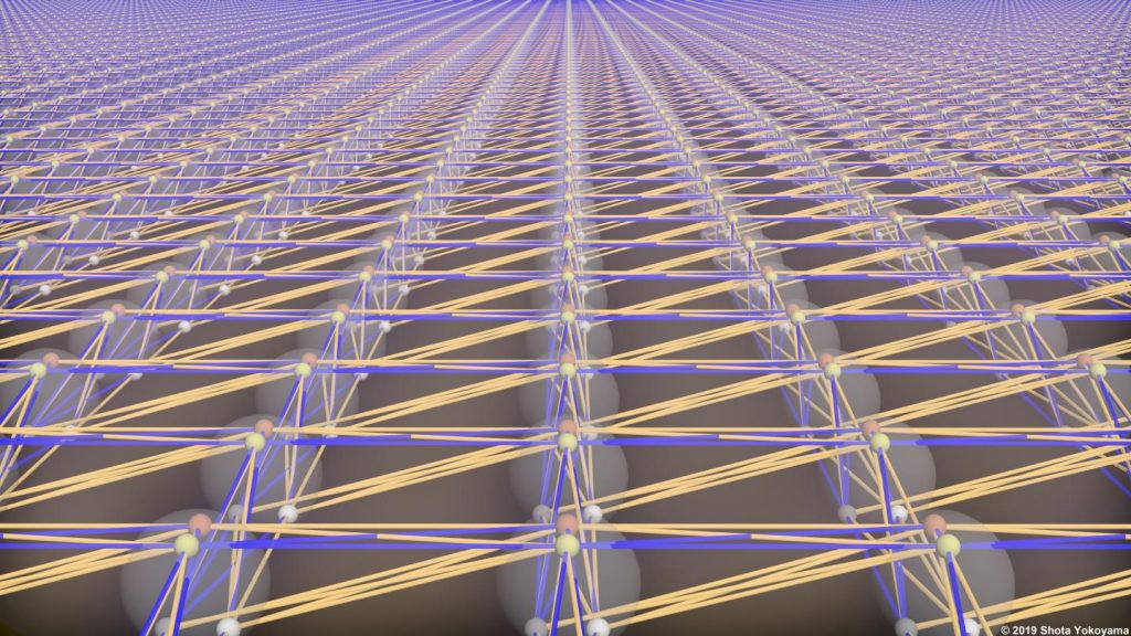
Memristor (or memory resistors) devices are non-volatile electronic memory devices that were first theorized by Leon Chua in the 1970’s. However, it was some thirty years later that the first practical device was fabricated. This was in 2008 when a group led by Stanley Williams at HP Research Labs realized that switching of the resistance between a conducting and less conducting state in metal-oxide thin-film devices was showing Leon Chua’s memristor behaviour.

The high interest in memristor devices also stems from the fact that these devices emulate the memory and learning properties of biological synapses. i.e. the electrical resistance value of the device is dependent on the history of the current flowing through it.

There is a huge effort underway to use memristor devices in neuromorphic computing applications and it is now reasonable to imagine the development of a new generation of artificial intelligent devices with very low power consumption (non-volatile), ultra-fast performance and high-density integration.

These discoveries come at an important juncture in microelectronics, since there is increasing disparity between computational needs of Big Data, Artificial Intelligence (A.I.) and the Internet of Things (IoT), and the capabilities of existing computers. The increases in speed, efficiency and performance of computer technology cannot continue in the same manner as it has done since the 1960s.

To date, most memristor research has focussed on the electronic switching properties of the device. However, for many applications it is useful to have an additional handle (or degree of freedom) on the device to control its resistive state. For example memory and processing in the brain also involves numerous chemical and bio-chemical reactions that control the brain structure and its evolution through development.

To emulate this in a simple solid-state system composed of just switches alone is not possible. In our research, we are interested in using light to mediate this essential control.

We have demonstrated that light can be used to make short and long-term memory and we have shown how light can modulate a special type of learning, called spike timing dependent plasticity (STDP). STDP involves two neuronal spikes incident across a synapse at the same time. Depending on the relative timing of the spikes and their overlap across the synaptic cleft, the connection strength is other strengthened or weakened.

In our earlier work, we were only able to achieve to small switching effects in memristors using light. In our latest work (Advanced Electronic Materials, “Percolation Threshold Enables Optical Resistive-Memory Switching and Light-Tuneable Synaptic Learning in Segregated Nanocomposites”), we take advantage of a percolating-like nanoparticle morphology to vastly increase the magnitude of the switching between electronic resistance states when light is incident on the device.

We have used an inhomogeneous percolating network consisting of metallic nanoparticles distributed in filamentary-like conduction paths. Electronic conduction and the resistance of the device is very sensitive to any disruption of the conduction path(s).

By embedding the nanoparticles in a polymer that can expand or contract with light the conduction pathways are broken or re-connected causing very large changes in the electrical resistance and memristance of the device.

Our devices could lead to the development of new memristor-based artificial intelligence systems that are adaptive and reconfigurable using a combination of optical and electronic signalling. Furthermore, they have the potential for the development of very fast optical cameras for artificial intelligence recognition systems.

Our work provides a nice proof-of-concept but the materials used means the optical switching is slow. The materials are also not well suited to industry fabrication. In our on-going work we are addressing these switching speed issues whilst also focussing on industry compatible materials.

Currently we are working on a new type of optical memristor device that should give us orders of magnitude improvement in the optical switching speeds whilst also retaining a large difference between the resistance on and off states. We hope to be able to achieve nanosecond switching speeds. The materials used are also compatible with industry standard methods of fabrication.

The new devices should also have applications in optical communications, interfacing and photonic computing. We are currently looking for commercial investors to help fund the research on these devices so that we can bring the device specifications to a level of commercial interest.

If you’re interested in memristors, Kemp’s article is well written and quite informative for nonexperts, assuming of course you can tolerate not understanding everything perfectly.

Here are links and citations for two papers. The first is the latest referred to in the article, a May 2019 paper and the second is a paper appearing in July 2019.

Percolation Threshold Enables Optical Resistive‐Memory Switching and Light‐Tuneable Synaptic Learning in Segregated Nanocomposites by Ayoub H. Jaafar, Mary O’Neill, Stephen M. Kelly, Emanuele Verrelli, Neil T. Kemp. Advanced Electronic Materials DOI: https://doi.org/10.1002/aelm.201900197 First published: 28 May 2019

Wavelength dependent light tunable resistive switching graphene oxide nonvolatile memory devices by Ayoub H.Jaafar, N.T.Kemp. DOI: https://doi.org/10.1016/j.carbon.2019.07.007 Carbon Available online 3 July 2019

The first paper (May 2019) is definitely behind a paywall and the second paper (July 2019) appears to be behind a paywall.

Dr. Kemp’s work has been featured here previously in a January 3, 2018 posting in the subsection titled, Shining a light on the memristor.

China

This work from China was announced in a June 20, 2019 news item on Nanowerk,

Memristors, demonstrated by solid-state devices with continuously tunable resistance, have emerged as a new paradigm for self-adaptive networks that require synapse-like functions. Spin-based memristors offer advantages over other types of memristors because of their significant endurance and high energy effciency.

However, it remains a challenge to build dense and functional spintronic memristors with structures and materials that are compatible with existing ferromagnetic devices. Ta/CoFeB/MgO heterostructures are commonly used in interfacial PMA-based [perpendicular magnetic anisotropy] magnetic tunnel junctions, which exhibit large tunnel magnetoresistance and are implemented in commercial MRAM [magnetic random access memory] products.

“To achieve the memristive function, DW is driven back and forth in a continuous manner in the CoFeB layer by applying in-plane positive or negative current pulses along the Ta layer, utilizing SOT that the current exerts on the CoFeB magnetization,” said Shuai Zhang, a coauthor in the paper. “Slowly propagating domain wall generates a creep in the detection area of the device, which yields a broad range of intermediate resistive states in the AHE [anomalous Hall effect] measurements. Consequently, AHE resistance is modulated in an analog manner, being controlled by the pulsed current characteristics including amplitude, duration, and repetition number.”

“For a follow-up study, we are working on more neuromorphic operations, such as spike-timing-dependent plasticity and paired pulsed facilitation,” concludes You. …

Here’s are links to and citations for the paper (Note: It’s a little confusing but I believe that one of the links will take you to the online version, as for the ‘open access’ link, keep reading),

A Spin–Orbit‐Torque Memristive Device by Shuai Zhang, Shijiang Luo, Nuo Xu, Qiming Zou, Min Song, Jijun Yun, Qiang Luo, Zhe Guo, Ruofan Li, Weicheng Tian, Xin Li, Hengan Zhou, Huiming Chen, Yue Zhang, Xiaofei Yang, Wanjun Jiang, Ka Shen, Jeongmin Hong, Zhe Yuan, Li Xi, Ke Xia, Sayeef Salahuddin, Bernard Dieny, Long You. Advanced Electronic Materials Volume 5, Issue 4 April 2019 (print version) 1800782 DOI: https://doi.org/10.1002/aelm.201800782 First published [online]: 30 January 2019 Note: there is another DOI, https://doi.org/10.1002/aelm.201970022 where you can have open access to Memristors: A Spin–Orbit‐Torque Memristive Device (Adv. Electron. Mater. 4/2019)

The paper published online in January 2019 is behind a paywall and the paper (almost the same title) published in April 2019 has a new DOI and is open access. Final note: I tried accessing the ‘free’ paper and opened up a free file for the artwork featuring the work from China on the back cover of the April 2019 of Advanced Electronic Materials.

Korea

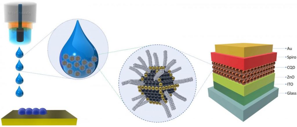
Usually when I see the words transparency and flexibility, I expect to see graphene is one of the materials. That’s not the case for this paper (link to and citation for),

Transparent and flexible photonic artificial synapse with piezo-phototronic modulator: Versatile memory capability and higher order learning algorithm by Mohit Kumar, Joondong Kim, Ching-Ping Wong. Nano Energy Volume 63, September 2019, 103843 DOI: https://doi.org/10.1016/j.nanoen.2019.06.039 Available online 22 June 2019

Here’s the abstract for the paper where you’ll see that the material is made up of zinc oxide silver nanowires,

An artificial photonic synapse having tunable manifold synaptic response can be an essential step forward for the advancement of novel neuromorphic computing. In this work, we reported the development of highly transparent and flexible two-terminal ZnO/Ag-nanowires/PET photonic artificial synapse [emphasis mine]. The device shows purely photo-triggered all essential synaptic functions such as transition from short-to long-term plasticity, paired-pulse facilitation, and spike-timing-dependent plasticity, including in the versatile memory capability. Importantly, strain-induced piezo-phototronic effect within ZnO provides an additional degree of regulation to modulate all of the synaptic functions in multi-levels. The observed effect is quantitatively explained as a dynamic of photo-induced electron-hole trapping/detraining via the defect states such as oxygen vacancies. We revealed that the synaptic functions can be consolidated and converted by applied strain, which is not previously applied any of the reported synaptic devices. This study will open a new avenue to the scientific community to control and design highly transparent wearable neuromorphic computing.

This paper is behind a paywall.

Bendable phones that are partially organic

It’s been about nine  or 10 years since I first heard about bendable phones (my September 29, 2010 posting). The concept keeps popping up from time to time (my April 25, 2017 posting) and this time, we have Australian scientists to thank for this latest work described in an October 5, 2018 news item on Nanowerk (Note: A link has been removed),

Engineers at ANU [Australian National University] have invented a semiconductor with organic and inorganic materials that can convert electricity into light very efficiently, and it is thin and flexible enough to help make devices such as mobile phones bendable (Advanced Materials, “Efficient and Layer-Dependent Exciton Pumping across Atomically Thin Organic–Inorganic Type-I Heterostructures”).

The invention also opens the door to a new generation of high-performance electronic devices made with organic materials that will be biodegradable or that can be easily recycled, promising to help substantially reduce e-waste.

An October 5, 2018 ANU press release (also on EurekAlert but published October 4, 2018) expands on the theme,

The huge volumes of e-waste generated by discarded electronic devices around the world is causing irreversible damage to the environment. Australia produces 200,000 tonnes of e-waste every year – only four per cent of this waste is recycled.

The organic component has the thickness of just one atom – made from just carbon and hydrogen – and forms part of the semiconductor that the ANU team developed. The inorganic component has the thickness of around two atoms. The hybrid structure can convert electricity into light efficiently for displays on mobile phones, televisions and other electronic devices.

Lead senior researcher Associate Professor Larry Lu said the invention was a major breakthrough in the field.

“For the first time, we have developed an ultra-thin electronics component with excellent semiconducting properties that is an organic-inorganic hybrid structure and thin and flexible enough for future technologies, such as bendable mobile phones and display screens,” said Associate Professor Lu from the ANU Research School of Engineering.

PhD researcher Ankur Sharma, who recently won the ANU 3-Minute Thesis competition, said experiments demonstrated the performance of their semiconductor would be much more efficient than conventional semiconductors made with inorganic materials such as silicon.

“We have the potential with this semiconductor to make mobile phones as powerful as today’s supercomputers,” said Mr Sharma from the ANU Research School of Engineering.

“The light emission from our semiconducting structure is very sharp, so it can be used for high-resolution displays and, since the materials are ultra-thin, they have the flexibility to be made into bendable screens and mobile phones in the near future.”

The team grew the organic semiconductor component molecule by molecule, in a similar way to 3D printing. The process is called chemical vapour deposition.

“We characterised the opto-electronic and electrical properties of our invention to confirm the tremendous potential of it to be used as a future semiconductor component,” Associate Professor Lu said.

“We are working on growing our semiconductor component on a large scale, so it can be commercialised in collaboration with prospective industry partners.”

Here’s a link to and a citation for the paper,

Efficient and Layer‐Dependent Exciton Pumping across Atomically Thin Organic–Inorganic Type‐I Heterostructures by Linglong Zhang, Ankur Sharma, Yi Zhu, Yuhan Zhang, Bowen Wang, Miheng Dong, Hieu T. Nguyen, Zhu Wang, Bo Wen, Yujie Cao, Boqing Liu, Xueqian Sun, Jiong Yang, Ziyuan Li. Advanced Materials Volume30, Issue 40 1803986 (October 4, 2018) DOI:https://doi.org/10.1002/adma.201803986 First published [onliine]: 30 August 2018

This paper is behind a paywall.

Probing the physical limits of plasmons in organic molecules with fewer than 50 atoms

A Sept. 5, 2018  news item on ScienceDaily introduces the work,

Rice University [Texas, US] researchers are probing the physical limits of excited electronic states called plasmons by studying them in organic molecules with fewer than 50 atoms.

A Sept. 4, 2018 Rice University news release (also on EurekAlert published on Sept. 5, 2018), which originated the news item, explains what plasmons are and why this research is being undertaken,

Plasmons are oscillations in the plasma of free electrons that constantly swirl across the surface of conductive materials like metals. In some nanomaterials, a specific color of light can resonate with the plasma and cause the electrons inside it to lose their individual identities and move as one, in rhythmic waves. Rice’s Laboratory for Nanophotonics (LANP) has pioneered a growing list of plasmonic technologies for applications as diverse as color-changing glass, molecular sensing, cancer diagnosis and treatment, optoelectronics, solar energy collection and photocatalysis.

Reporting online in the Proceedings of the National Academy of Sciences, LANP scientists detailed the results of a two-year experimental and theoretical study of plasmons in three different polycyclic aromatic hydrocarbons (PAHs). Unlike the plasmons in relatively large metal nanoparticles, which can typically be described with classical electromagnetic theory like Maxwell’s [James Clerk Maxwell] equations, the paucity of atoms in the PAHs produces plasmons that can only be understood in terms of quantum mechanics, said study co-author and co-designer Naomi Halas, the director of LANP and the lead researcher on the project.

“These PAHs are essentially scraps of graphene that contain five or six fused benzene rings surrounded by a perimeter of hydrogen atoms,” Halas said. “There are so few atoms in each that adding or removing even a single electron dramatically changes their electronic behavior.”

Halas’ team had experimentally verified the existence of molecular plasmons in several previous studies. But an investigation that combined side by side theoretical and experimental perspectives was needed, said study co-author Luca Bursi, a postdoctoral research associate and theoretical physicist in the research group of study co-designer and co-author Peter Nordlander.

“Molecular excitations are a ubiquity in nature and very well studied, especially for neutral PAHs, which have been considered as the standard of non-plasmonic excitations in the past,” Bursi said. “Given how much is already known about PAHs, they were an ideal choice for further investigation of the properties of plasmonic excitations in systems as small as actual molecules, which represent a frontier of plasmonics.”

Lead co-author Kyle Chapkin, a Ph.D. student in applied physics in the Halas research group, said, “Molecular plasmonics is a new area at the interface between plasmonics and molecular chemistry, which is rapidly evolving. When plasmonics reach the molecular scale, we lose any sharp distinction of what constitutes a plasmon and what doesn’t. We need to find a new rationale to explain this regime, which was one of the main motivations for this study.”

In their native state, the PAHs that were studied — anthanthrene, benzo[ghi]perylene and perylene — are charge-neutral and cannot be excited into a plasmonic state by the visible wavelengths of light used in Chapkin’s experiments. In their anionic form, the molecules contain an additional electron, which alters their “ground state” and makes them plasmonically active in the visible spectrum. By exciting both the native and anionic forms of the molecules and comparing precisely how they behaved as they relaxed back to their ground states, Chapkin and Bursi built a solid case that the anionic forms do support molecular plasmons in the visible spectrum.

The key, Chapkin said, was identifying a number of similarities between the behavior of known plasmonic particles and the anionic PAHs. By matching both the timescales and modes for relaxation behaviors, the LANP team built up a picture of a characteristic dynamics of low-energy plasmonic excitations in the anionic PAHs.

“In molecules, all excitations are molecular excitations, but select excited states show some characteristics that allow us to draw a parallel with the well-established plasmonic excitations in metal nanostructures,” Bursi said.

“This study offers a window on the sometimes surprising behavior of collective excitations in few-atom quantum systems,” Halas said. “What we’ve learned here will aid our lab and others in developing quantum-plasmonic approaches for ultrafast color-changing glass, molecular-scale optoelectronics and nonlinear plasmon-mediated optics.”

Here’s a link to and a citation for the paper,

Lifetime dynamics of plasmons in the few-atom limit by Kyle D. Chapkin, Luca Bursi, Grant J. Stec, Adam Lauchner, Nathaniel J. Hogan, Yao Cui, Peter Nordlander, and Naomi J. Halas. PNAS September 11, 2018 115 (37) 9134-9139; published ahead of print August 27, 2018 DOI: https://doi.org/10.1073/pnas.1805357115

This paper is behind a paywall.

Build nanoparticles using techniques from the ancient Egyptians

Great Pyramid of Giza and Sphinx [downloaded from http://news.ifmo.ru/en/science/photonics/news/7731/]

Russian and German scientists have taken a closer look at the Great Pyramid as they investigate better ways of designing sensors and solar cells. From a July 30, 2018 news item on Nanowerk,

An international research group applied methods of theoretical physics to investigate the electromagnetic response of the Great Pyramid to radio waves. Scientists predicted that under resonance conditions the pyramid can concentrate electromagnetic energy in its internal chambers and under the base. The research group plans to use these theoretical results to design nanoparticles capable of reproducing similar effects in the optical range. Such nanoparticles may be used, for example, to develop sensors and highly efficient solar cells.

A July 30, 2018 ITMO University press release, which originated the news item,  expands on the theme,

While Egyptian pyramids are surrounded by many myths and legends, we have little scientifically reliable information about their physical properties. As it turns out, sometimes this information proves to be more fascinating than any fiction. This idea found confirmation in a new joint study undertaken by scientists from ITMO University and the Laser Zentrum Hannover. The physicists took an interest in how the Great Pyramid would interact with electromagnetic waves of a proportional, or resonant, length. Calculations showed that in the resonant state the pyramid can concentrate electromagnetic energy in its internal chambers as well as under its base, where the third unfinished chamber is located.

These conclusions were derived on the basis of numerical modeling and analytical methods of physics. The researchers first estimated that resonances in the pyramid can be induced by radio waves with a length ranging from 200 to 600 meters. Then they made a model of the electromagnetic response of the pyramid and calculated the extinction cross section. This value helps to estimate which part of the incident wave energy can be scattered or absorbed by the pyramid under resonant conditions. Finally, for the same conditions, the scientists obtained the electromagnetic fields distribution inside the pyramid.

3D model of the pyramid. Credit: cheops.SU

In order to explain the results, the scientists conducted a multipole analysis. This method is widely used in physics to study the interaction between a complex object and electromagnetic field. The object scattering the field is replaced by a set of simpler sources of radiation: multipoles. The collection of multipoles radiation coincides with the field scattering by an entire object. Therefore, by knowing the type of each multipole, it is possible to predict and explain the distribution and configuration of the scattered fields in the whole system.

The Great Pyramid attracted the researchers’ attention while they were studying the interaction between light and dielectric nanoparticles. The scattering of light by nanoparticles depends on their size, shape, and refractive index of the source material. By varying these parameters, it is possible to determine the resonance scattering regimes and use them to develop devices for controlling light at the nanoscale.

“Egyptian pyramids have always attracted great attention. We as scientists were interested in them as well, and so we decided to look at the Great Pyramid as a particle resonantly dissipating radio waves. Due to the lack of information about the physical properties of the pyramid, we had to make some assumptions. For example, we assumed that there are no unknown cavities inside, and the building material has the properties of an ordinary limestone and is evenly distributed in and out of the pyramid. With these assumptions, we obtained interesting results that can have important practical applications,” says Andrey Evlyukhin, DSc, scientific supervisor and coordinator of the research.

Now the scientists plan to use the results to reproduce similar effects at the nanoscale.

Polina Kapitanova
Polina Kapitanova

“By choosing a material with suitable electromagnetic properties, we can obtain pyramidal nanoparticles with a potential for practical application in nanosensors and effective solar cells,” says Polina Kapitanova, PhD, associate at the Faculty of Physics and Engineering of ITMO University.

The research was supported by the Russian Science Foundation and the Deutsche Forschungsgemeinschaft (grants № 17-79-20379 and №16-12-10287).

Here’s a link to and a citation for the paper,

Electromagnetic properties of the Great Pyramid: First multipole resonances and energy concentration featured by Mikhail Balezin, Kseniia V. Baryshnikova, Polina Kapitanova, and Andrey B. Evlyukhin. Journal of Applied Physics 124, 034903 (2018) https://doi.org/10.1063/1.5026556 or Journal of Applied Physics, Volume 124, Issue 3. 10.1063/1.5026556 Published Online 20 July 2018

This paper is behind a paywall..

Manipulating light at the nanoscale with kiragami-inspired technique

At left, different patterns of slices through a thin metal foil, are made by a focused ion beam. These patterns cause the metal to fold up into predetermined shapes, which can be used for such purposes as modifying a beam of light. Courtesy of the researchers

Nanokiragami (or nano-kiragami) is a fully fledged field of research? That was news to me as was much else in a July 6, 2018 news item on ScienceDaily,

Nanokirigami has taken off as a field of research in the last few years; the approach is based on the ancient arts of origami (making 3-D shapes by folding paper) and kirigami (which allows cutting as well as folding) but applied to flat materials at the nanoscale, measured in billionths of a meter.

Now, researchers at MIT [Massachusetts Institute of Technology] and in China have for the first time applied this approach to the creation of nanodevices to manipulate light, potentially opening up new possibilities for research and, ultimately, the creation of new light-based communications, detection, or computational devices.

A July 6, 2018 MIT news release (also on EurekAlert), which originated the news item, adds detail,

The findings are described today [July 6, 2018] in the journal Science Advances, in a paper by MIT professor of mechanical engineering Nicholas X Fang and five others. Using methods based on standard microchip manufacturing technology, Fang and his team used a focused ion beam to make a precise pattern of slits in a metal foil just a few tens of nanometers thick. The process causes the foil to bend and twist itself into a complex three-dimensional shape capable of selectively filtering out light with a particular polarization.

Previous attempts to create functional kirigami devices have used more complicated fabrication methods that require a series of folding steps and have been primarily aimed at mechanical rather than optical functions, Fang says. The new nanodevices, by contrast, can be formed in a single folding step and could be used to perform a number of different optical functions.

For these initial proof-of-concept devices, the team produced a nanomechanical equivalent of specialized dichroic filters that can filter out circularly polarized light that is either “right-handed” or “left-handed.” To do so, they created a pattern just a few hundred nanometers across in the thin metal foil; the result resembles pinwheel blades, with a twist in one direction that selects the corresponding twist of light.

The twisting and bending of the foil happens because of stresses introduced by the same ion beam that slices through the metal. When using ion beams with low dosages, many vacancies are created, and some of the ions end up lodged in the crystal lattice of the metal, pushing the lattice out of shape and creating strong stresses that induce the bending.

“We cut the material with an ion beam instead of scissors, by writing the focused ion beam across this metal sheet with a prescribed pattern,” Fang says. “So you end up with this metal ribbon that is wrinkling up” in the precisely planned pattern.

“It’s a very nice connection of the two fields, mechanics and optics,” Fang says. The team used helical patterns to separate out the clockwise and counterclockwise polarized portions of a light beam, which may represent “a brand new direction” for nanokirigami research, he says.

The technique is straightforward enough that, with the equations the team developed, researchers should now be able to calculate backward from a desired set of optical characteristics and produce the needed pattern of slits and folds to produce just that effect, Fang says.

“It allows a prediction based on optical functionalities” to create patterns that achieve the desired result, he adds. “Previously, people were always trying to cut by intuition” to create kirigami patterns for a particular desired outcome.

The research is still at an early stage, Fang points out, so more research will be needed on possible applications. But these devices are orders of magnitude smaller than conventional counterparts that perform the same optical functions, so these advances could lead to more complex optical chips for sensing, computation, or communications systems or biomedical devices, the team says.

For example, Fang says, devices to measure glucose levels often use measurements of light polarity, because glucose molecules exist in both right- and left-handed forms which interact differently with light. “When you pass light through the solution, you can see the concentration of one version of the molecule, as opposed to the mixture of both,” Fang explains, and this method could allow for much smaller, more efficient detectors.

Circular polarization is also a method used to allow multiple laser beams to travel through a fiber-optic cable without interfering with each other. “People have been looking for such a system for laser optical communications systems” to separate the beams in devices called optical isolaters, Fang says. “We have shown that it’s possible to make them in nanometer sizes.”

The team also included MIT graduate student Huifeng Du; Zhiguang Liu, Jiafang Li (project supervisor), and Ling Lu at the Chinese Academy of Sciences in Beijing; and Zhi-Yuan Li at the South China University of Technology. The work was supported by the National Key R&D Program of China, the National Natural Science Foundation of China, and the U.S Air Force Office of Scientific Research.

The researchers have also provided some GIFs,

And,

Here’s a link to and a citation for the paper,

Nano-kirigami with giant optical chirality by Zhiguang Liu, Huifeng Du, Jiafang Li, Ling Lu, Zhi-Yuan Li, and Nicholas X. Fang. Science Advances 06 Jul 2018: Vol. 4, no. 7, eaat4436 DOI: 10.1126/sciadv.aat4436

This paper is open access.